Electromagnetic shield structure for electronic device

a shield structure and electronic device technology, applied in the direction of casings with display/control units, electric apparatus casings/cabinets/drawers, localised screening, etc., can solve the problems of difficult space security, noise generation of the hardware supporting respective functions, and limit in space allocation, so as to enhance the mounting and wiring efficiency of components

Active Publication Date: 2016-08-18
SAMSUNG ELECTRONICS CO LTD
View PDF26 Cites 24 Cited by
  • Summary
  • Abstract
  • Description
  • Claims
  • Application Information

AI Technical Summary

Benefits of technology

[0013]Another aspect of the present disclosure is to provide an electromagnetic shield structure for an electronic device, which is capable of securing a performance of suppressing ElectroStatic Discharge (ESD) / ElectroMagnetic Interference (EMI) while enhancing component mounting and wiring efficiency within a limited PCB space. In accordance with an aspect of the present disclosure, an electronic device is provided, which includes a printed circuit board (PCB) including a first surface, a second surface, and a side surface; an electronic component arranged on the first surface, adjacent to a portion of the side surface; a shield structure including a cap that covers the electronic component and a sidewall extending from a periphery of the cap toward the first surface of the PCB, wherein the sidewall extends in a first direction that is non-parallel to the first surface of the PCB; a first conductive structure that is formed on a portion of the side surface of the PCB; and a second conductive structure that is formed on a portion of the first surface to be connected to the first conductive structure. The sidewall contacts with the first surface of the PCB and overlaps with the second conductive structure, when viewed from above the first surface of the PCB.

Problems solved by technology

In addition, when a plurality of chips and components are mounted on a PCB, hardware for supporting respective functions may generate noise while performing a switching operation for data processing.
The generated noise acts as noise to other processor chips therearound.
However, as the electronic devices, which support the communication function, are slimmed, the bezels of the electronic devices are minimized, and as other additional pieces of hardware are mounted, it becomes difficult to secure a space, such as a component mounting space or a wiring space, and there is a limit in space allocation.
The space allocation puts a lot of pressure either from a design standpoint of electronic devices or a technology standpoint of electronic devices.

Method used


Image

  • Electromagnetic shield structure for electronic device
  • Electromagnetic shield structure for electronic device
  • Electromagnetic shield structure for electronic device

Examples


Embodiment Construction

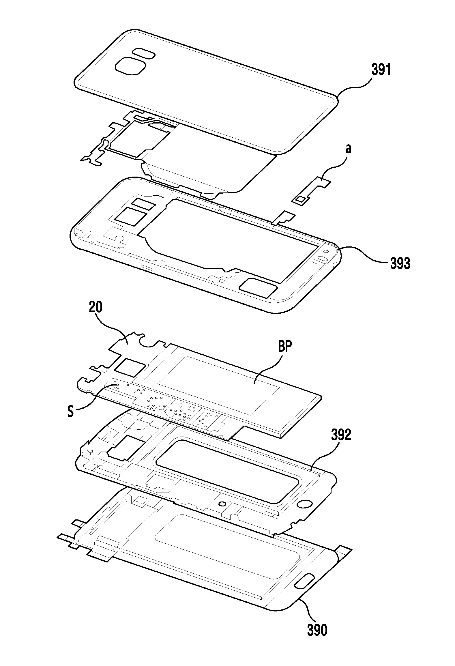
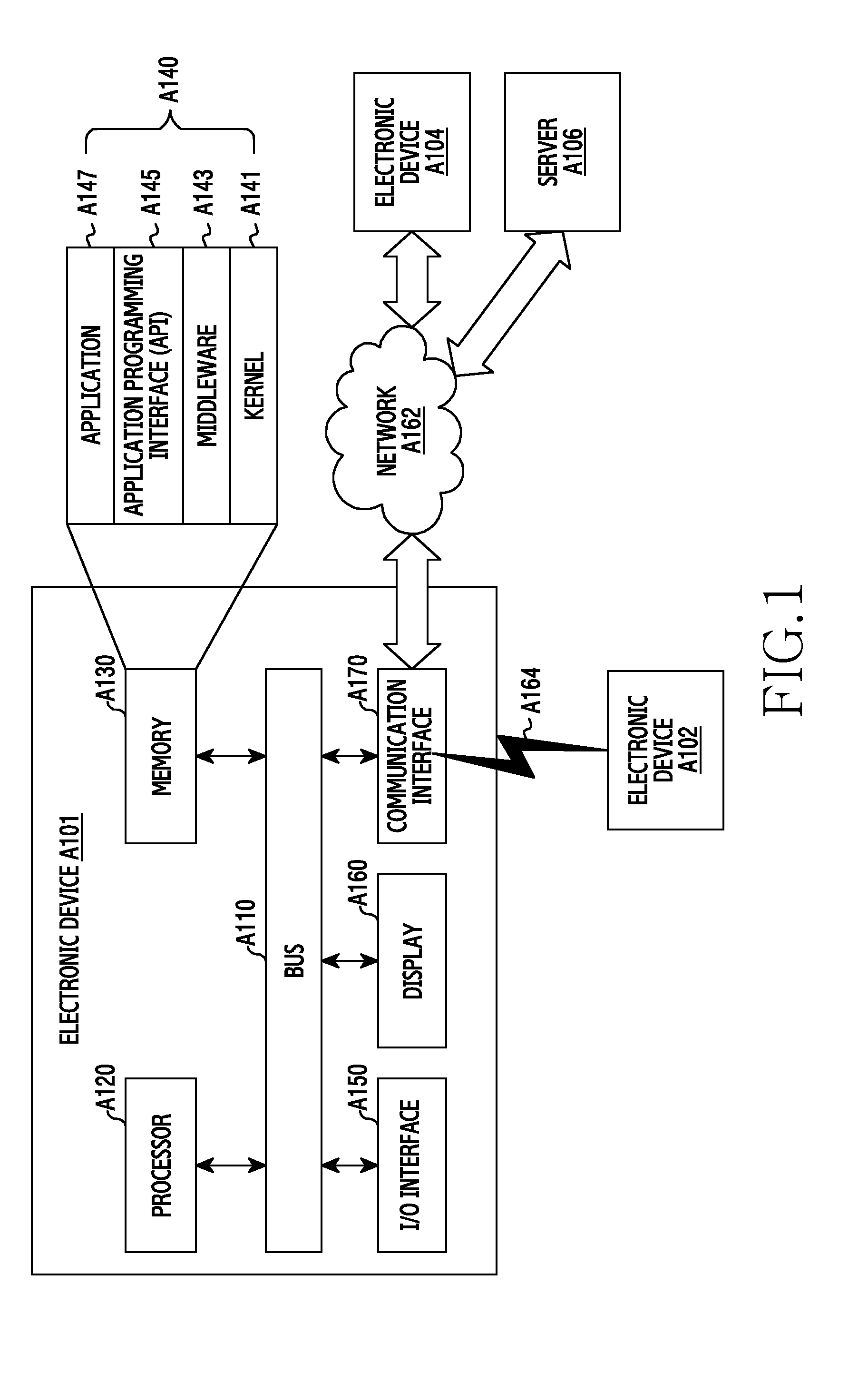
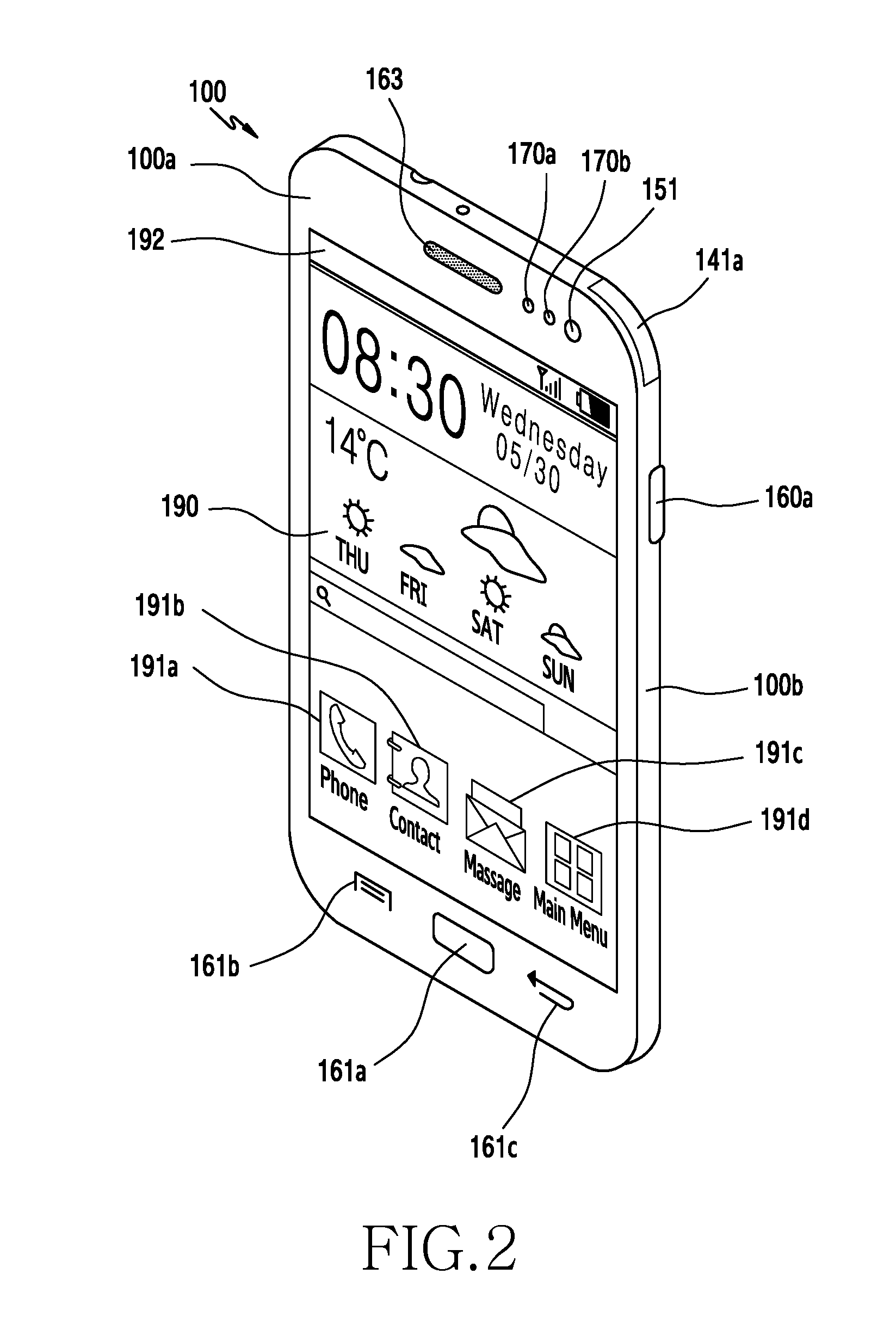
[0073]Hereinafter, various embodiments of the present disclosure will be described with reference to the accompanying drawings. Although specific embodiments of the present disclosure are illustrated in the drawings and relevant detailed descriptions are provided, various changes can be made and various embodiments may be provided. Accordingly, various embodiments of the present disclosure are not limited to the specific embodiments and should be construed as including all changes and / or equivalents or substitutes included in the ideas and technological scopes of embodiments of the present disclosure.

[0074]In the explanation of the drawings, similar reference numerals are used for similar elements.

[0075]Herein, the terms “include” or “may include” may indicate the presence of disclosed corresponding functions, operations, elements, etc., but do not limit the presence of additional one or more functions, operations, elements, etc. In addition, the terms “include” or “have” indicate t...


PUM


Abstract

An electronic device is provided that includes a PCB including a first surface, a second surface, and a side surface; an electronic component arranged on the first surface, adjacent to a portion of the side surface; a shield structure including a cap that covers the electronic component and a sidewall extending from a periphery of the cap toward the first surface of the PCB, wherein the sidewall extends in a first direction that is non-parallel to the first surface of the PCB; a first conductive structure that is formed on a portion of the side surface of the PCB; and a second conductive structure that is formed on a portion of the first surface to be connected to the first conductive structure. The sidewall contacts with the first surface of the PCB and overlaps with the second conductive structure, when viewed from above the first surface of the PCB.

Description

PRIORITY[0001]This application claims priority under 35 U.S.C. §119(a) to Korean Application Serial No. 10-2015-0024499, which was filed in the Korean Intellectual Property Office on Feb. 17, 2015, the entire content of which is incorporated herein by reference.BACKGROUND[0002]1. Field of the Invention[0003]The present disclosure relates generally to an electromagnetic structure for an electronic device.[0004]2. Description of the Related Art[0005]Electronic devices include various pieces of hardware that are integrated on a Printed Circuit Board (PCB) in order to support various functions. For example, a terminal, which supports a mobile communication function, includes a communication chip for supporting the mobile communication function and a processor chip for supporting a multimedia function, both of which are integrated on a PCB. In addition, a processor chip for supporting a touch screen, and various modules for supporting user functions, such as a broadcasting reception modu...

Claims


Application Information

Patent Timeline
Patent Type & Authority Applications(United States)
IPC IPC(8): H05K9/00H05K5/00
CPCH05K9/002H05K5/0004H05K5/0017H05K1/0218H05K2201/10371H05K9/0024H05K9/0039H05K2201/0919H05K2201/09354H05K1/0259H05K2201/0715H01L2224/16225H05K9/0028H05K9/0032
Inventor PARK, JUNG-SIKCHOI, SEUNG-KIHEO, JOONHONG, HYUN-JU
Owner SAMSUNG ELECTRONICS CO LTD
Why Eureka
Try Eureka