Display device with touch sensor

a display device and touch sensor technology, applied in the field of touch sensor display devices, can solve the problems of reducing display quality, difficult connections, increasing thickness of display devices, etc., and achieve the effect of preventing the lowering of display quality and high precision

Inactive Publication Date: 2016-09-01
SHARP KK
View PDF5 Cites 30 Cited by
  • Summary
  • Abstract
  • Description
  • Claims
  • Application Information

AI Technical Summary

Benefits of technology

[0035]An embodiment of the present invention provides a display device with a touch sensor with a high precision, of which the display quality is prevented from being lowered by the touch sensor electrode.

Problems solved by technology

However, with such a display device, the thickness of the display device increases by the thickness of the touch panel substrate, and the display quality will be lowered because of a decrease in transmittance due to the touch panel substrate.
Moreover, the terminal provision area of the touch panel substrate is separate from that of the display device, thereby making connections difficult.
This is to address problems, such as the provision of touch sensor electrodes inside the liquid crystal display device, which complicates the display device manufacturing process, the touch sensor electrodes affecting the display quality, the inability to increase the driving frequency, thereby limiting the realization of large-size products.

Method used


Image

  • Display device with touch sensor
  • Display device with touch sensor
  • Display device with touch sensor

Examples


embodiment 1

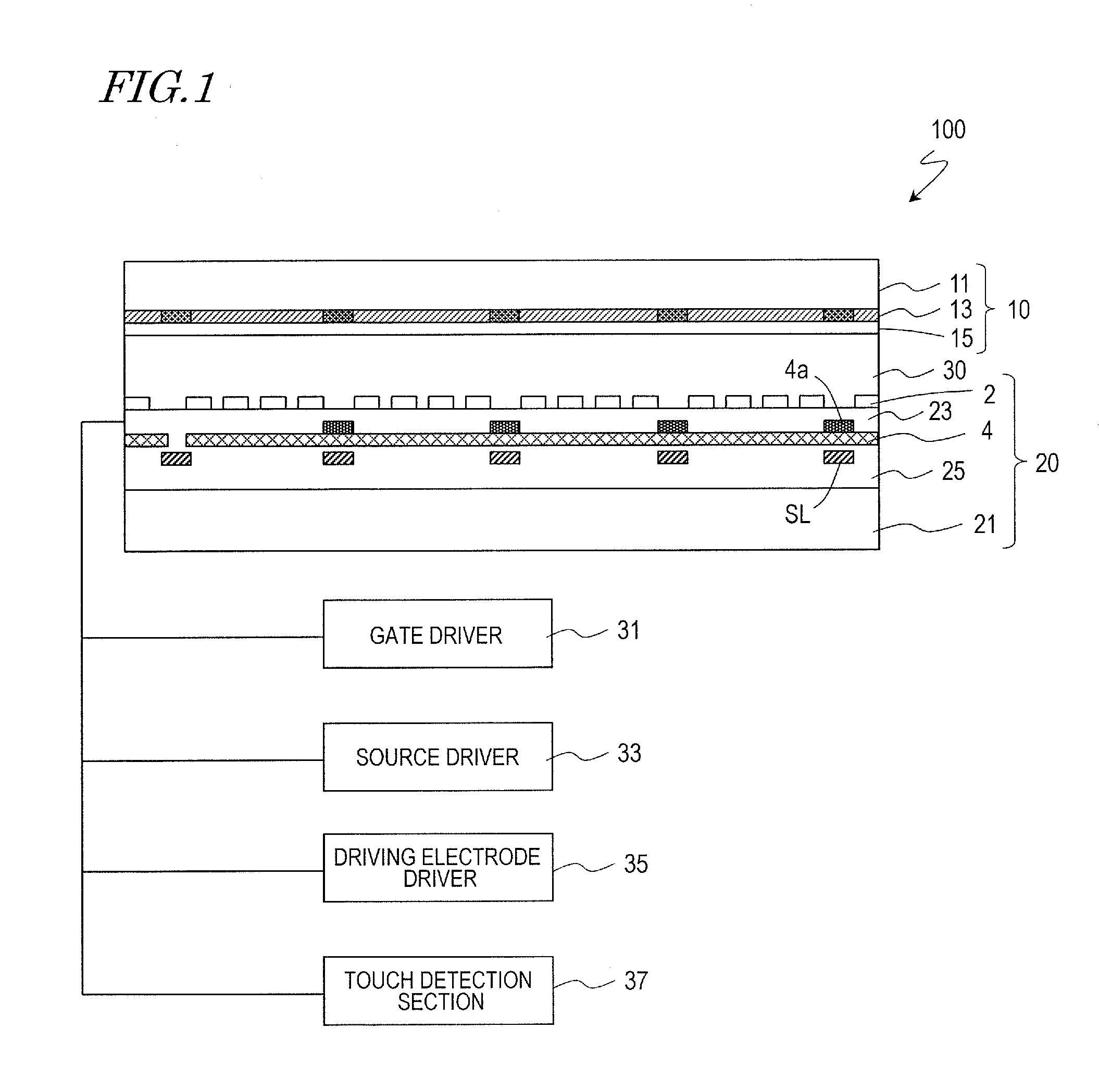
[0068]FIG. 1 is a diagram showing a display device 100 with a touch sensor according to an embodiment of the present invention. The display device 100 with a touch sensor includes a TFT substrate (pixel substrate) 20, a counter substrate 10 provided on the observer side of the TFT substrate 20, and a liquid crystal layer 30 provided between the TFT substrate 20 and the counter substrate 10.

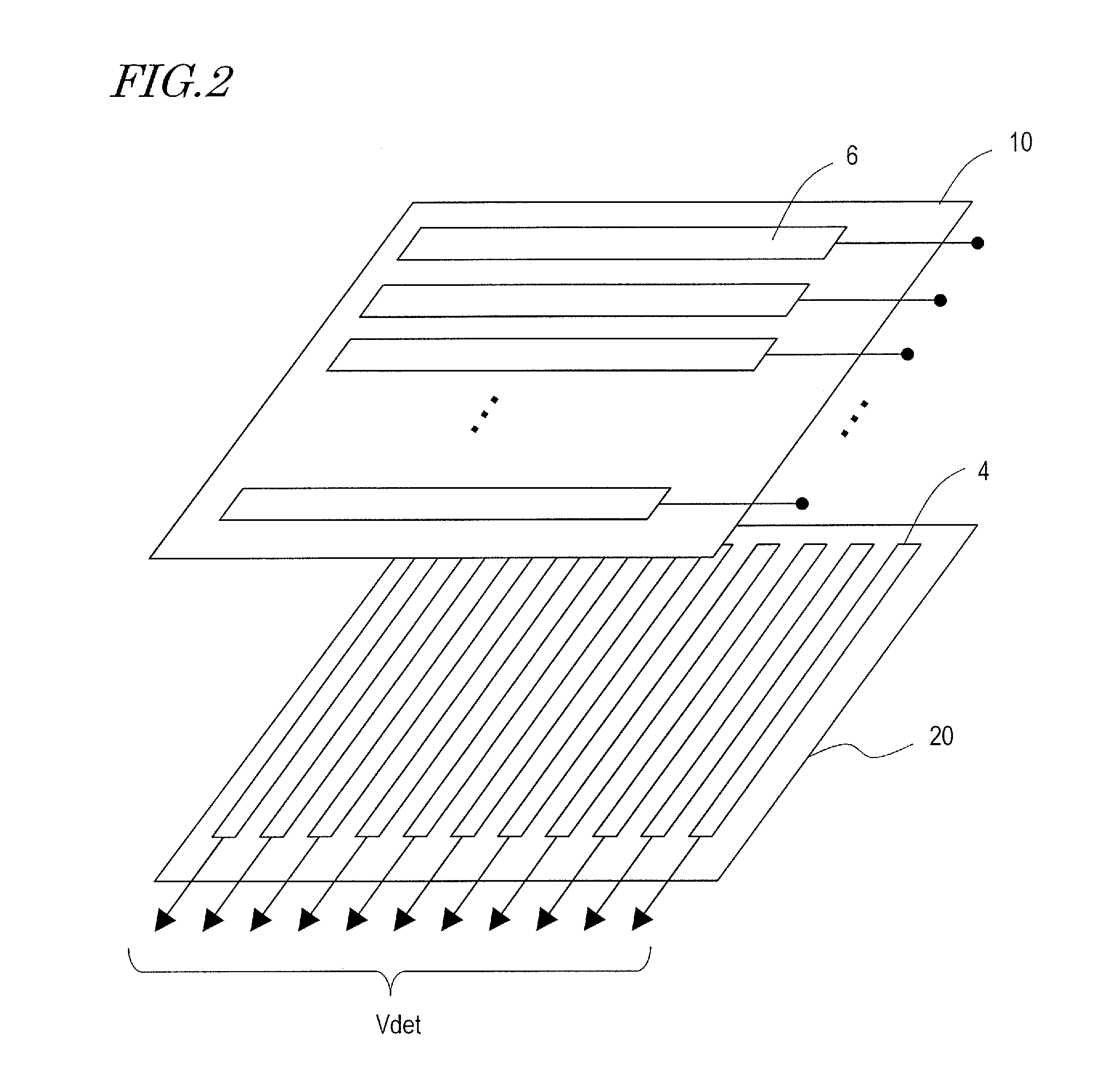
[0069]The TFT substrate 20 includes a glass substrate 21, and a pixel electrode 2 and a common electrode 4 for applying a voltage across the liquid crystal layer 30. An insulating layer 25 is provided between the glass substrate 21 and the common electrode 4, and an insulating layer 23 is provided between the common electrode 4 and the pixel electrode 2. The common electrode 4 is used also as a detection electrode of the touch sensor.

[0070]The counter substrate 10 includes a glass substrate 11, a color filter layer 13 and a resin layer 15. A driving electrode 6 (FIG. 3) of the touch sensor is prov...

embodiment 2

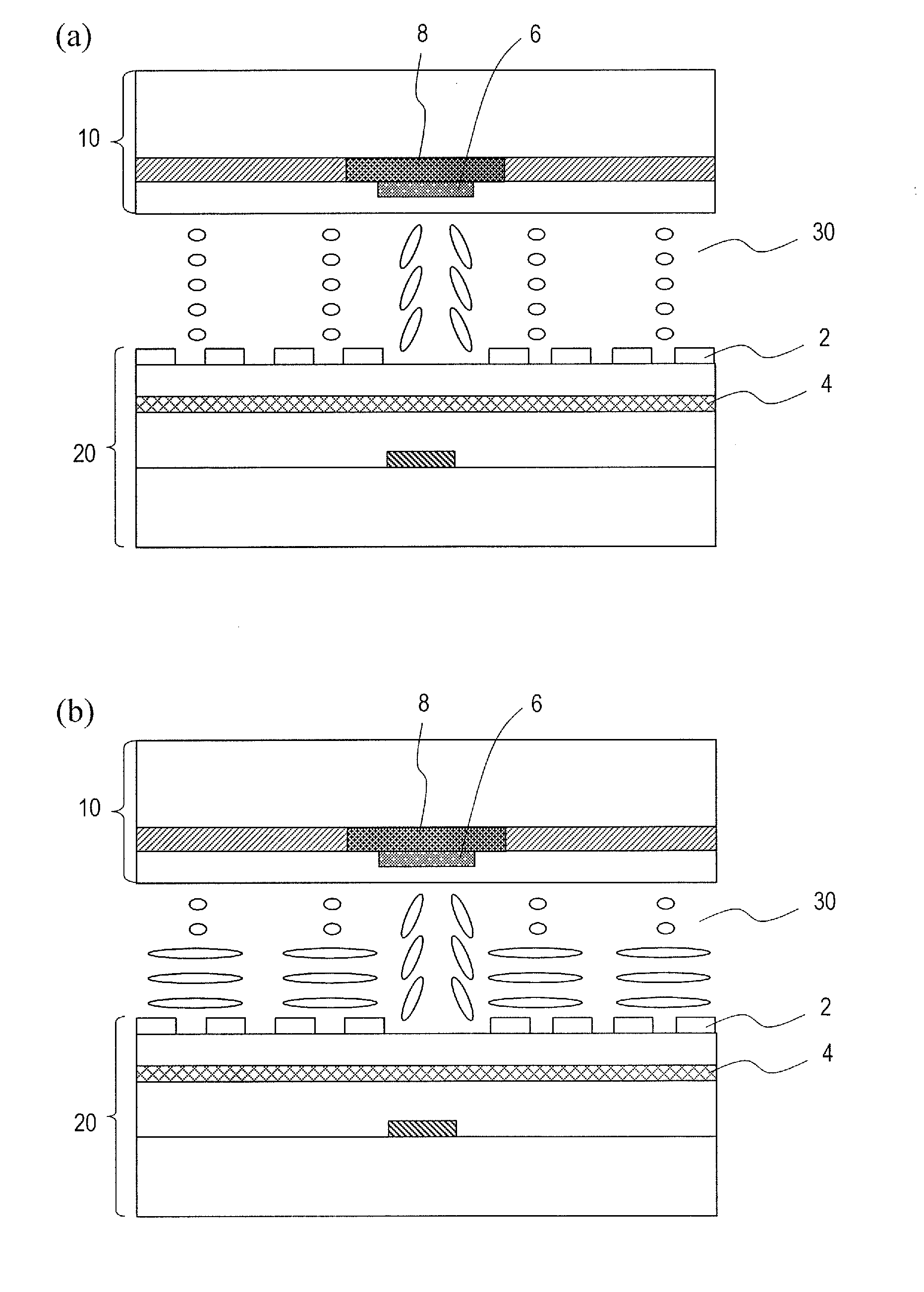
[0105]Next, a display device 100 with a touch sensor according to Embodiment 2 of the present invention will be described. FIG. 17 is a diagram showing the TFT substrate 20 of the display device 100 with a touch sensor of the present embodiment, FIG. 18(a) is a cross-sectional view taken along line AA′ shown in FIG. 17, and FIG. 18(b) is a cross-sectional view taken along line BB′ shown in FIG. 17.

[0106]In this example, the common electrode 4 is provided closer to the liquid crystal layer 30 than the pixel electrode 2. Since the pixel electrode 2 is absent between the driving electrode 6 of the touch sensor and the detection electrode (common electrode) 4, the touch-detecting operation is not influenced by variations, among different liquid crystal displays, in the capacitance between the pixel electrode 2 and the common electrode 4. Thus, it is possible to increase the precision of the touch-detecting operation by the output voltage Vout shown in FIG. 11(b).

embodiment 3

[0107]Next, a display device 100 with a touch sensor according to Embodiment 3 of the present invention will be described. FIG. 19 is a diagram showing the TFT substrate 20 of the display device 100 with a touch sensor of the present embodiment, FIG. 20(a) is a cross-sectional view taken along line AA′ shown in FIG. 19, and FIG. 20(b) is a cross-sectional view taken along line BB′ shown in FIG. 19.

[0108]In this example, the driving electrode 6 is provided on the liquid crystal layer side of the resin layer 15, which is provided on the color filter layer 13. A portion 4C of the pattern of the detection electrode (common electrode) 4, opposing the driving electrode 6, is removed. That is, an area of the detection electrode on the TFT substrate side that overlaps the driving electrode, as seen in a plan view, is removed by patterning, thereby making it possible to reduce the capacity load with the driving electrode 6. After the surface is planarized by providing the resin layer 15 on t...


PUM

PropertyMeasurementUnit
sheet resistanceaaaaaaaaaa
sizeaaaaaaaaaa
widthaaaaaaaaaa

Abstract

A display device with a touch sensor (100) according to an embodiment of the present invention includes: a pixel substrate (20) including a plurality of pixel electrodes (2); a counter substrate (10) opposing the pixel substrate (20); a black matrix (8) extending in a first direction and in a second direction different from the first direction; and a touch sensor electrode (6) extending in the first direction. In a plan view where the counter substrate (10) is seen from a direction vertical to a planar direction of the counter substrate (10), a width in the second direction of a line of the black matrix (8) extending in the first direction is larger than a width in the first direction of a line of the black matrix (8) extending in the second direction; a width (W1) in the second direction of a line of the touch sensor electrode (6) extending in the first direction is smaller than a width (W2) in the second direction of the line of the black matrix (8) extending in the first direction; and the line of the touch sensor electrode (6) extending in the first direction and the line of the black matrix (8) extending in the first direction overlap each other.

Description

TECHNICAL FIELD[0001]The present invention relates to a display device with a touch sensor, and particularly to a display device with a touch sensor of a capacitive type.BACKGROUND ART[0002]In recent years, display devices having a touch panel function of a capacitive type, which can be operated intuitively and which is capable of multi-point detection, have been drawing public attention. However, with such a display device, the thickness of the display device increases by the thickness of the touch panel substrate, and the display quality will be lowered because of a decrease in transmittance due to the touch panel substrate. Moreover, the terminal provision area of the touch panel substrate is separate from that of the display device, thereby making connections difficult.[0003]As a mode to solve these problems, in-cell-type touch panels have been under discussion, in which the touch sensor function is incorporated into the liquid crystal display device itself. This is to address p...

Claims


Application Information

Patent Timeline
Patent Type & Authority Applications(United States)
IPC IPC(8): G06F3/041G02F1/1362G02F1/1343G06F3/044
CPCG06F3/0416G06F3/044G06F3/0412G06F2203/04111G02F1/134336G06F2203/04103G02F1/136209G06F3/0446G06F3/04166G06F3/0445G06F3/041
Inventor TADA, KENSHIOGAWA, HIROYUKISUGITA, YASUHIROYAMAGISHI, SHINJIMUGIRANEZA, JEAN
Owner SHARP KK
Why Eureka
Try Eureka