Organic light emitting diode display

a light-emitting diode and display technology, applied in the field of display devices, can solve problems such as new pixel defects and generation of pixel defects

Active Publication Date: 2016-09-08
SAMSUNG DISPLAY CO LTD
View PDF5 Cites 60 Cited by
  • Summary
  • Abstract
  • Description
  • Claims
  • Application Information

AI Technical Summary

Benefits of technology

[0012]According to aspects of embodiments of the present invention, instances of short circuits with an overlying conductive layer in an organic light emitting diode display may be prevented or reduced even in instances where there is an over-deposition of conductive material when forming a connection bridge with a data line.
[0022]According to aspects of some embodiments of the present invention, by forming the cutout in an anode, when forming a detour path by using a connection bridge, even though metal or conductive material of the detour path may be over-deposited, instances of a short circuit between the over-deposited material and the anode of the organic light emitting diode display may be reduced or prevented.

Problems solved by technology

Pixel defects may be generated due to a characteristic deviation of a transistor and a capacitor provided in each pixel or a short or a disconnection of wirings.
Such protrusions due to the over-deposition may increase the possibility of a short circuit with other metals or conductive materials such as the pixel electrode positioned on the connection bridge, thereby causing a new pixel defect.

Method used


Image

  • Organic light emitting diode display
  • Organic light emitting diode display
  • Organic light emitting diode display

Examples


Embodiment Construction

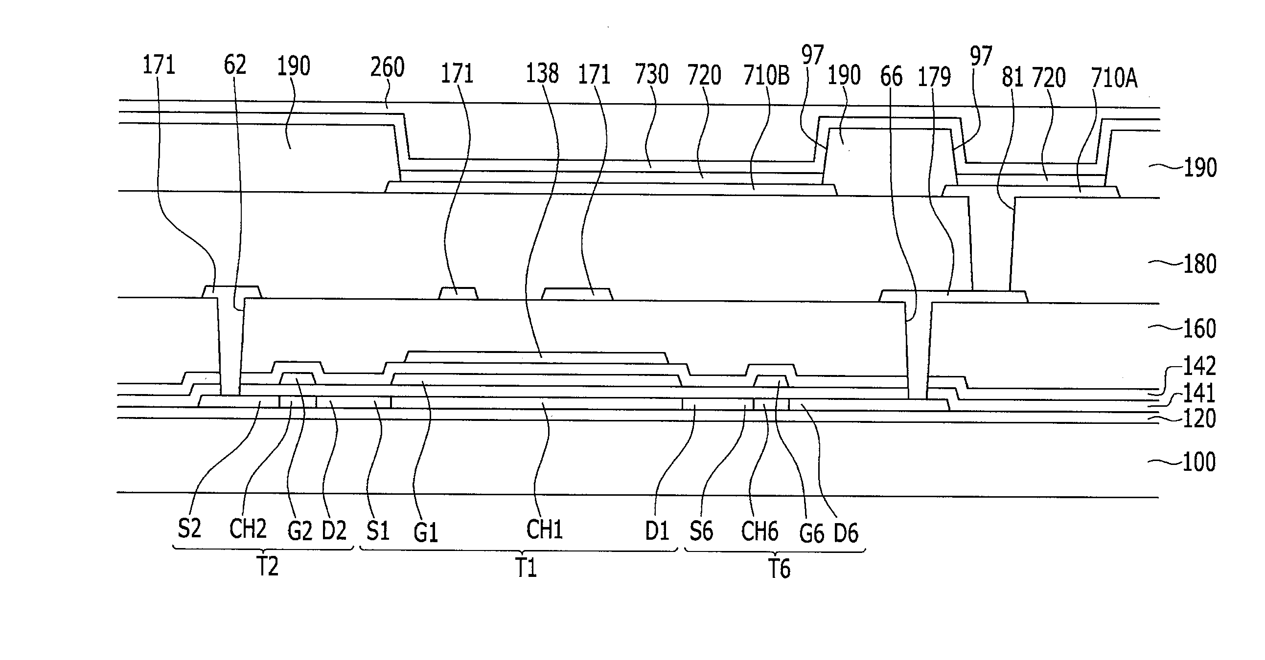
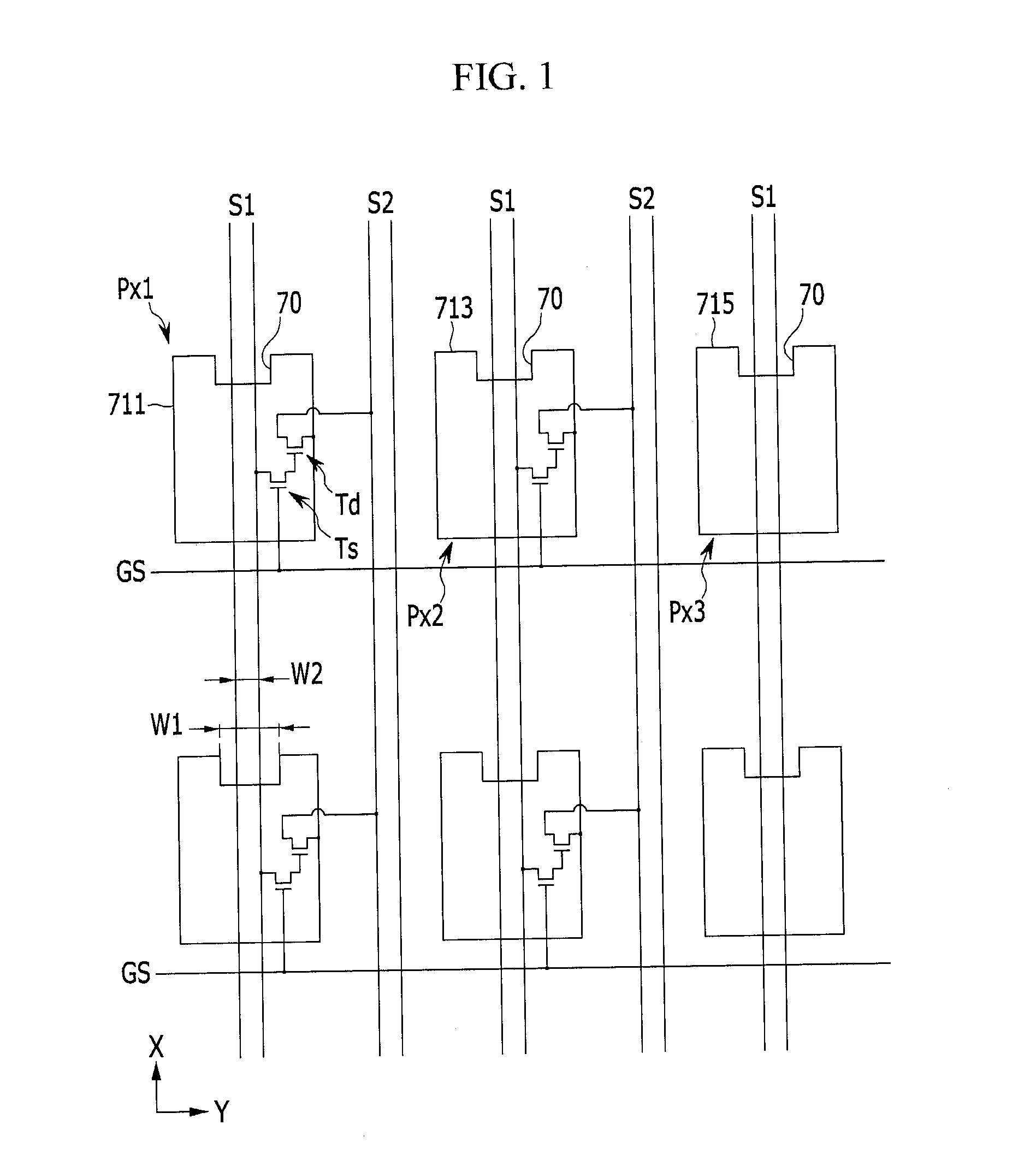
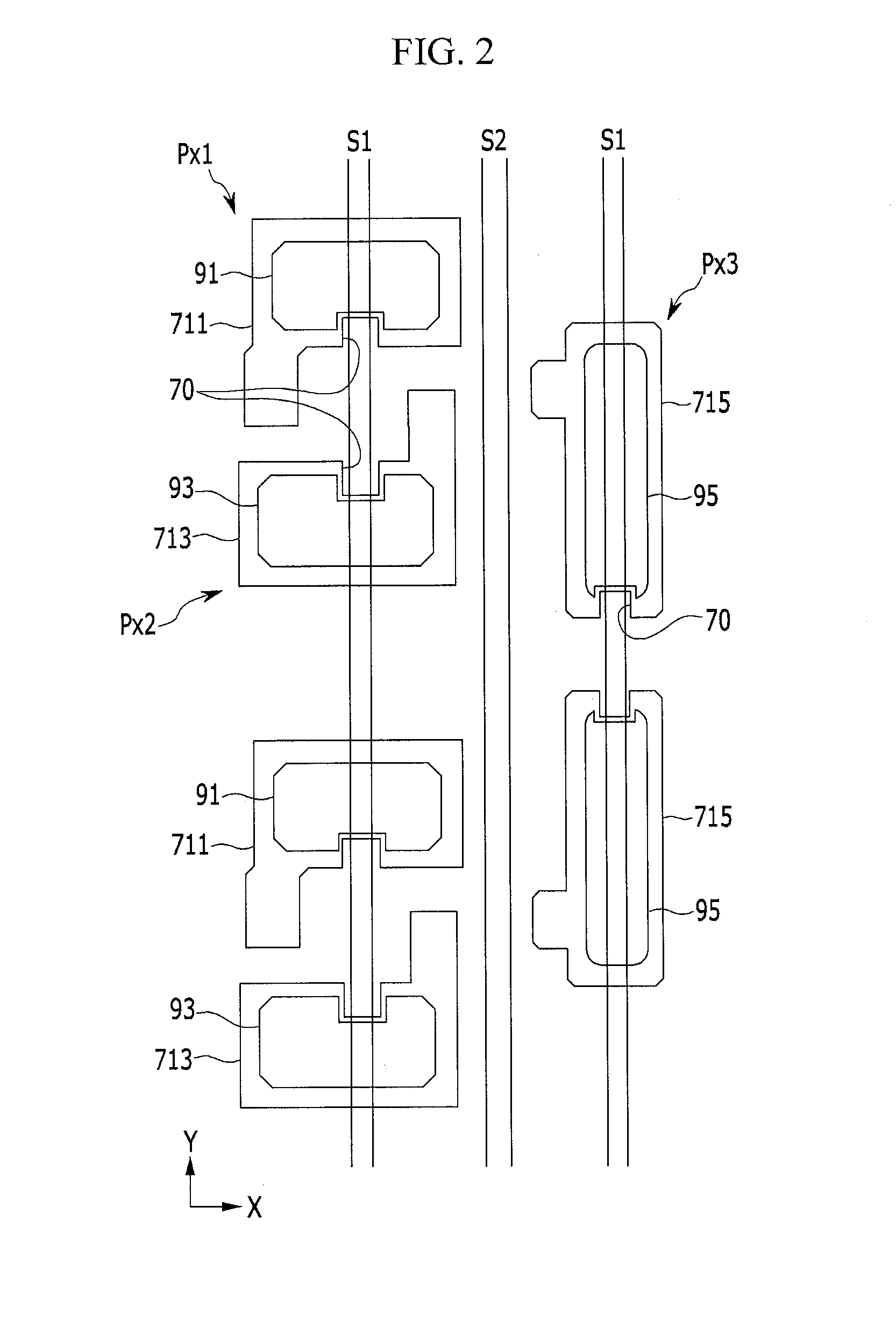
[0032]Several example embodiments according to the present invention are described hereinafter in detail with reference to the accompanying drawings in order to be easily understood by a person of ordinary skill in the art. The present invention can be embodied in several different forms, and is not limited to the example embodiments that are described herein.

[0033]In order to clarify the present invention, some aspects of the invention that are not connected with the description will be omitted, and the same elements or equivalents are referred to by the same reference numerals throughout the specification.

[0034]In addition, the size and thickness of each element shown in the drawings are arbitrarily shown for better understanding and ease of description, but the present invention is not limited thereto. In the drawings, the thickness of layers, films, panels, regions, etc., are exaggerated for clarity. In the drawings, for better understanding and ease of description, the thicknes...


PUM


Abstract

An organic light emitting diode display according to an example embodiment of the present invention includes: a substrate; a scan line and a data line that are insulated from one another and crossing each other on the substrate; a first transistor on the substrate and connected to the scan line and the data line; a second transistor connected to the first transistor; a first electrode connected to the second transistor and having a cutout; an organic emission layer on the first electrode; and a second electrode on the organic emission layer, wherein the cutout is at a position corresponding to the data line.

Description

CROSS-REFERENCE TO RELATED APPLICATION[0001]This application claims priority to and the benefit of Korean Patent Application No. 10-2015-0030561, filed in the Korean Intellectual Property Office on Mar. 4, 2015, the entire content of which is incorporated herein by reference.BACKGROUND[0002]1. Field[0003]Aspects of embodiments of the present invention relate to a display device.[0004]2. Description of the Related Art[0005]An organic light emitting diode display includes two electrodes and an organic light emitting layer positioned there between. Electrons injected from a cathode that is an electrode and holes injected from an anode that is another electrode are bonded to each other in the organic light emitting layer to form excitons. Light is emitted when the excitons discharge energy.[0006]Organic light emitting diode displays include a plurality of pixels including an organic light emitting diode formed of the cathode, the anode, and the organic light emitting layer. A plurality ...

Claims


Application Information

Patent Timeline
Patent Type & Authority Applications(United States)
IPC IPC(8): H01L27/32H01L51/52
CPCH01L27/3276H01L2251/301H01L51/5203H01L27/3246G09G3/3266G09G3/3275H10K59/352H10K59/353H10K59/121H10K59/122H10K59/131H10K50/813H10K2102/341H10K71/861H10K59/80515H10K59/12H10K59/35H10K59/1213H10K2102/00H10K2102/311
Inventor KIM, YONG CHULSO, DONG-YOONKIM, TAE GON
Owner SAMSUNG DISPLAY CO LTD
Why Eureka
Try Eureka