Nanostructured chip and method of producing the same

Active Publication Date: 2016-09-29
GLOBALWAFERS CO LTD
View PDF6 Cites 0 Cited by
  • Summary
  • Abstract
  • Description
  • Claims
  • Application Information

AI Technical Summary

Benefits of technology

[0006]In view of the above, the primary objective of the present invention is to provide a nanostructured chip and a method of p

Problems solved by technology

Consequently, the epitaxial layer might have cracks or bowings because the silicon substrate is too brittle to eliminate the stress, which may lead to a low yield in the subsequent processing procedures and even wafer fragmentation

Method used


Image

  • Nanostructured chip and method of producing the same
  • Nanostructured chip and method of producing the same
  • Nanostructured chip and method of producing the same

Examples


Example

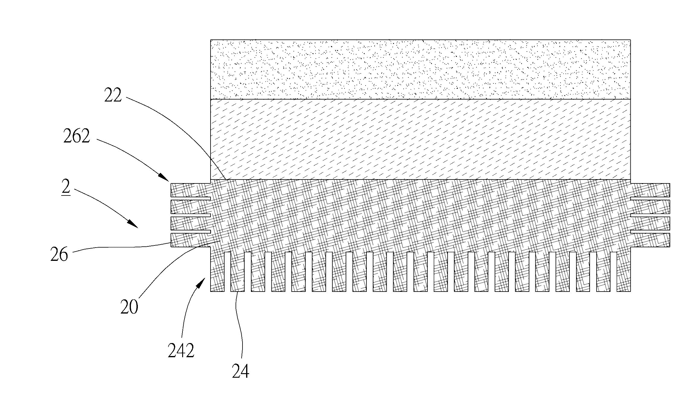
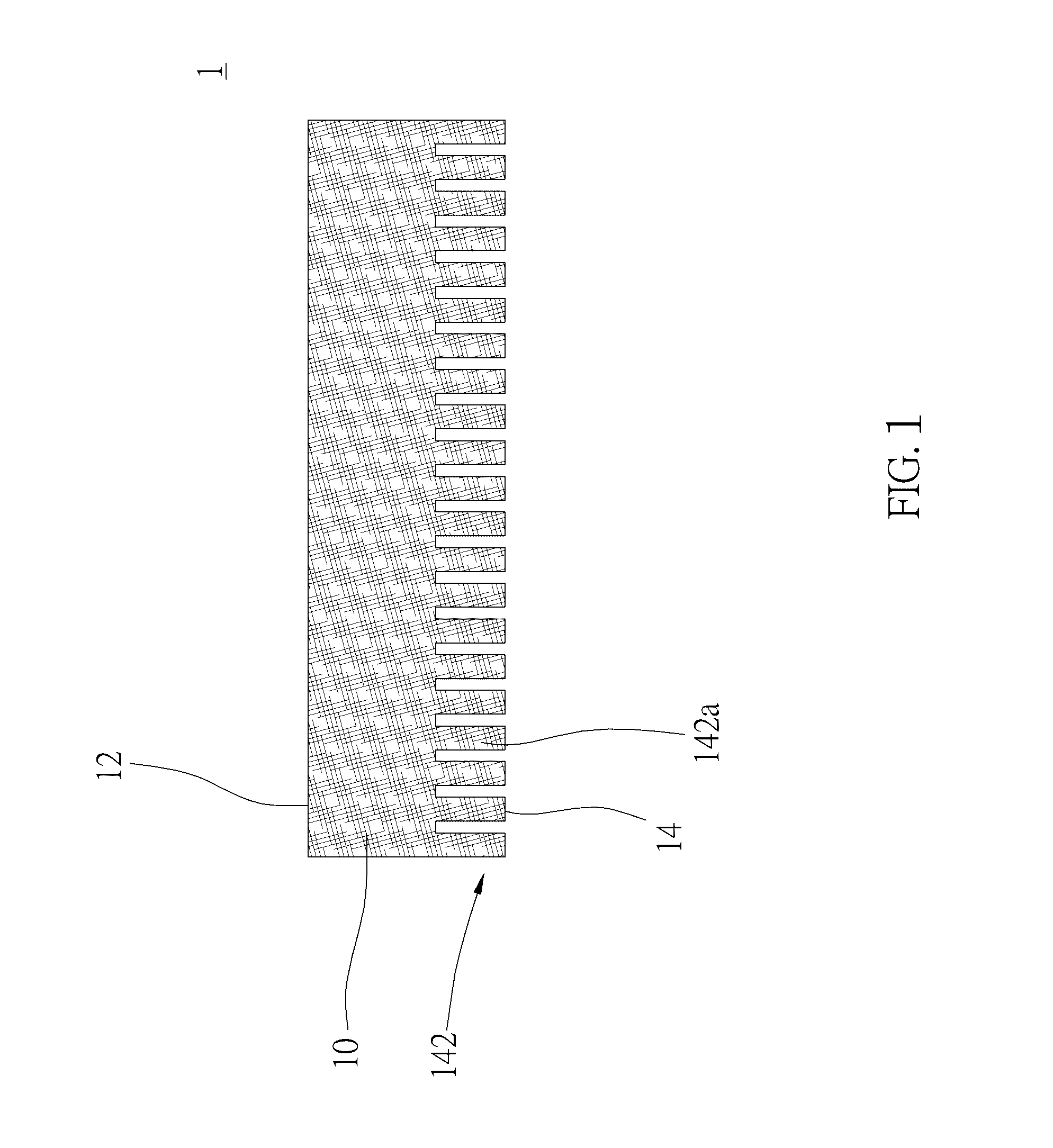
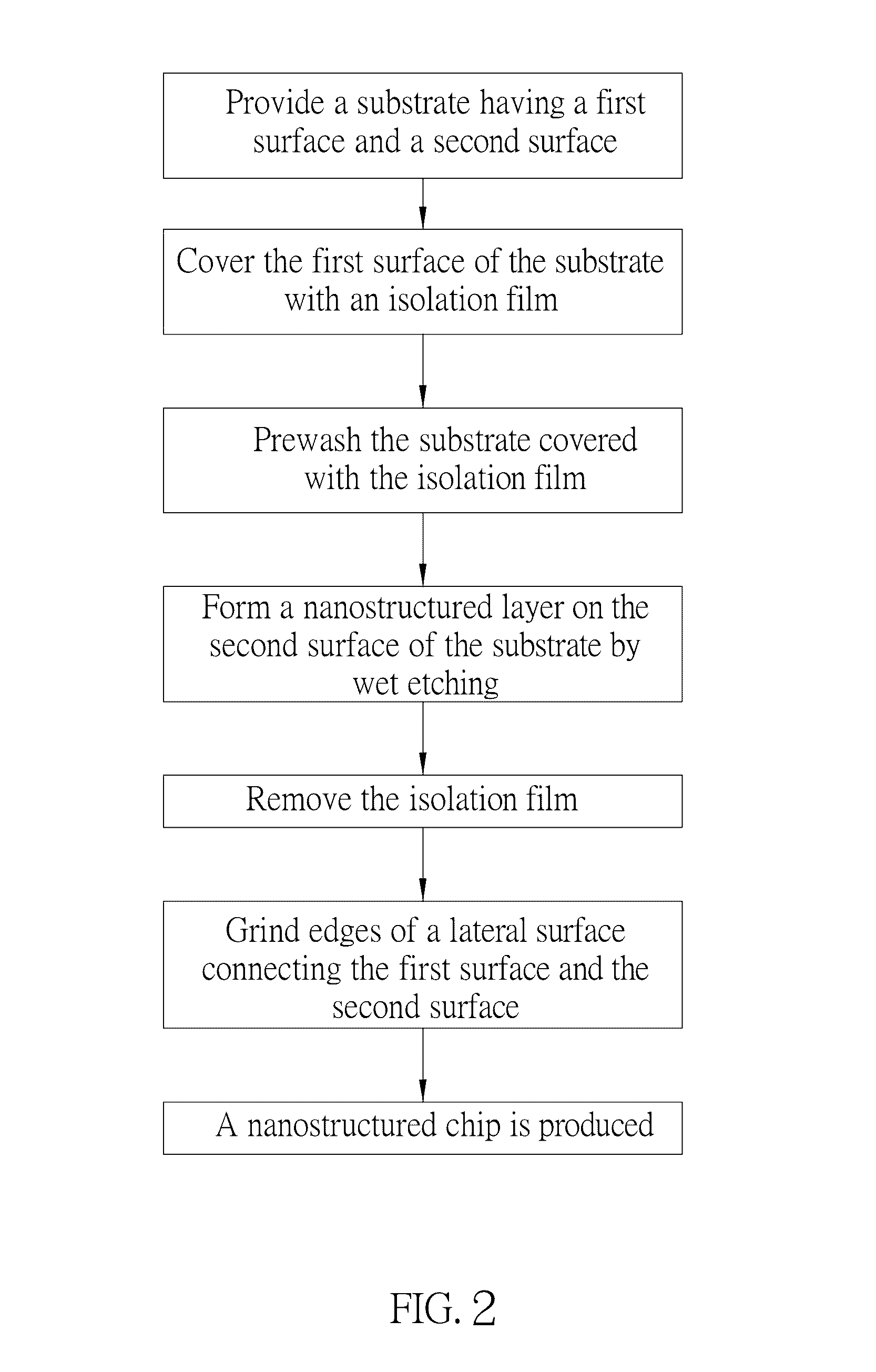
[0023]A nanostructured chip 1 shown in FIG. 1 is produced by a method shown in FIG. 2 including steps below.

[0024]Provide a substrate 10 having a first surface 12 and a second surface 14 which is opposite to the first surface 12. In the first preferred embodiment, the substrate 10 is a silicon substrate.

[0025]Cover the first surface 12 of the substrate 10 with a protective layer which is an isolation film in the first preferred embodiment.

[0026]Prewash the substrate 10 covered with the isolation film to the second surface 14 of the substrate 10 clean.

[0027]Form a nanostructured layer 142 on the second surface 14 by wet etching. In the first preferred embodiment, the substrate 10 is soaked in etching agent composed of hydrofluoric acid (HF), water, and silver nitrate (AgNO3) at a ratio of 1:4:1 for 40 minutes to form the nanostructured layer 142 including a plurality of nanopillars 142a which are illustrated in FIG. 3.

[0028]Remove the isolation film and wash the substrate, and next, ...


PUM


Abstract

A nanostructured chip includes a substrate and a nanostructured layer, wherein the substrate has a first surface and a second surface on which the nanostructured layer is formed. A method of producing the nanostructured chip includes the step of forming the nanostructured layer on the second surface of the substrate. Whereby, the nanostructured layer effectively disperses a stress to increase the flexural strength of the nanostructured chip. Therefore, during the subsequent procedures to form an epitaxial layer on the first surface, the nanostructured layer is helpful to prevent the epitaxial layer from generating cracks, and prevent the substrate from bowings, or fragments.

Description

BACKGROUND OF THE INVENTION[0001]1. Technical Field[0002]The present invention relates generally to chip production, and more particularly to a nanostructured chip and a method of producing the nanostructured chip.[0003]2. Description of Related Art[0004]In a conventional manufacturing process of a wafer, an epitaxial layer is formed on a surface of a substrate in advance, and is then processed to form particular structures or circuits.[0005]However, if the material of the substrate is different from that of the epitaxial layer (e.g., a silicon substrate with a gallium nitride (GaN) epitaxial layer formed thereon), a stress tends to be generated in the wafer during a cooling process due to the different thermal expansion coefficients between the substrate and the epitaxial layer. Consequently, the epitaxial layer might have cracks or bowings because the silicon substrate is too brittle to eliminate the stress, which may lead to a low yield in the subsequent processing procedures and...

Claims


Application Information

Patent Timeline
IPC IPC(8): H01L23/00H01L21/306H01L29/20H01L29/06
CPCH01L23/562H01L29/2003H01L21/30604H01L29/0673H01L21/02381H01L21/0243H01L21/02458H01L21/0254H01L21/02658H01L29/0657H01L29/0676
Inventor YEH, JER-LIANGCHUANG, CHIH-YUANFAN, CHUN-ISUN, CHIEN-JENSHIH, YING-RUHSU, WEN-CHING
Owner GLOBALWAFERS CO LTD
Why Eureka
Try Eureka