Semiconductor light emitting device, transfer head of semiconductor light emitting device, and method of transferring semiconductor light emitting device

a technology which is applied in the field transfer head of semiconductor light emitting device, can solve the problems of difficult implementation of flexibility for lcds, short life span, and slow response time, and achieve the effect of larger grip force and high reliability

Active Publication Date: 2016-10-13
LG ELECTRONICS INC
View PDF9 Cites 38 Cited by
  • Summary
  • Abstract
  • Description
  • Claims
  • Application Information

AI Technical Summary

Benefits of technology

[0008]Therefore, an aspect of the detailed description is to provide a novel method of transferring semiconductor light emitting devices with a higher reliability. More specifically, the present invention is to provide a method of transferring a semiconductor light emitting device with a larger grip force, and a transfer device.

Problems solved by technology

However, there exist problems such as a slow response time, difficult implementation of flexibility for LCDs, and there exist drawbacks such as short life span, poor yield as well as low flexibility for AMOLEDs.
However, the transfer process is inefficient and results in a poor yield and low reliability.

Method used


Image

  • Semiconductor light emitting device, transfer head of semiconductor light emitting device, and method of transferring semiconductor light emitting device
  • Semiconductor light emitting device, transfer head of semiconductor light emitting device, and method of transferring semiconductor light emitting device
  • Semiconductor light emitting device, transfer head of semiconductor light emitting device, and method of transferring semiconductor light emitting device

Examples


Embodiment Construction

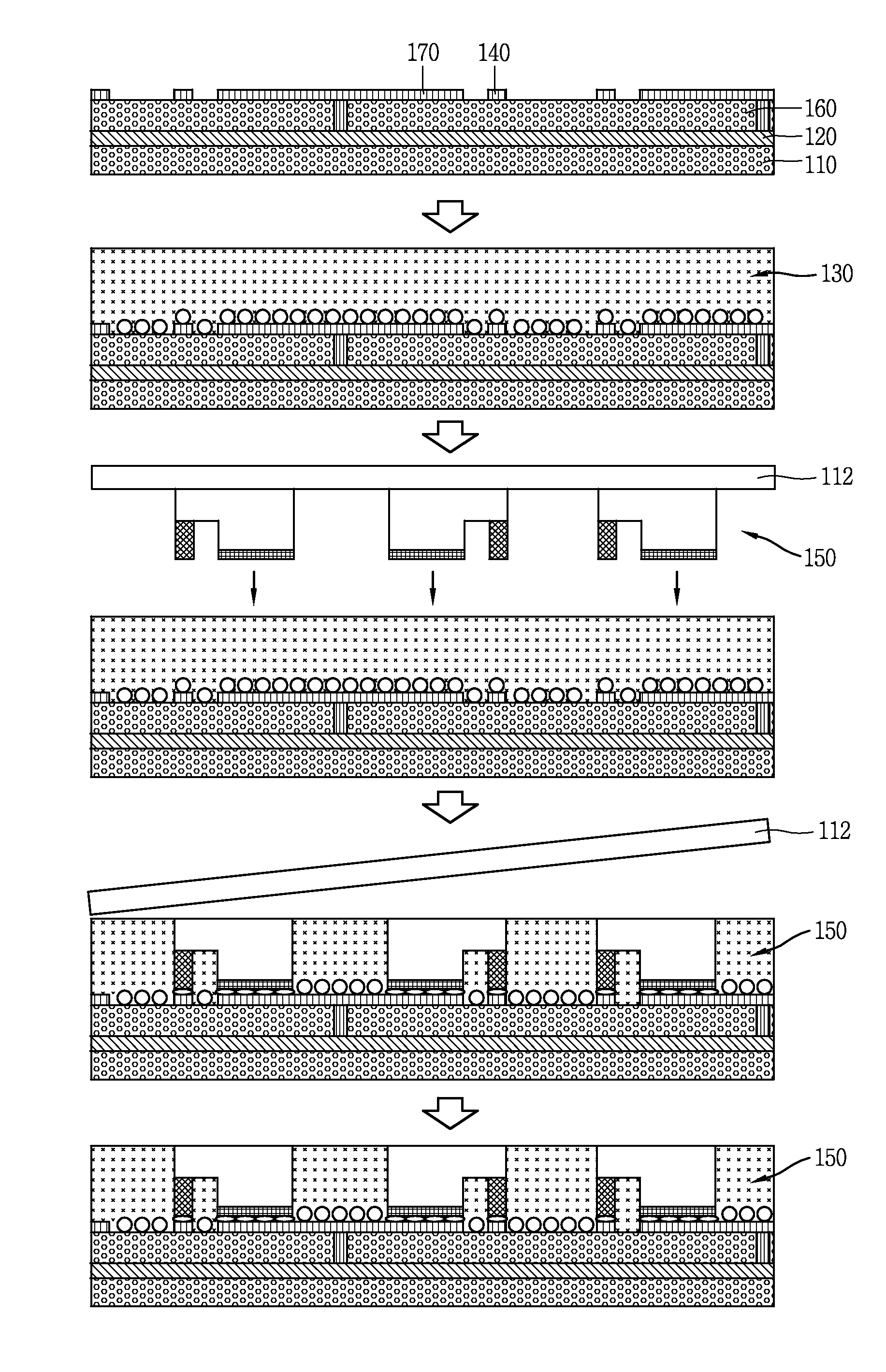
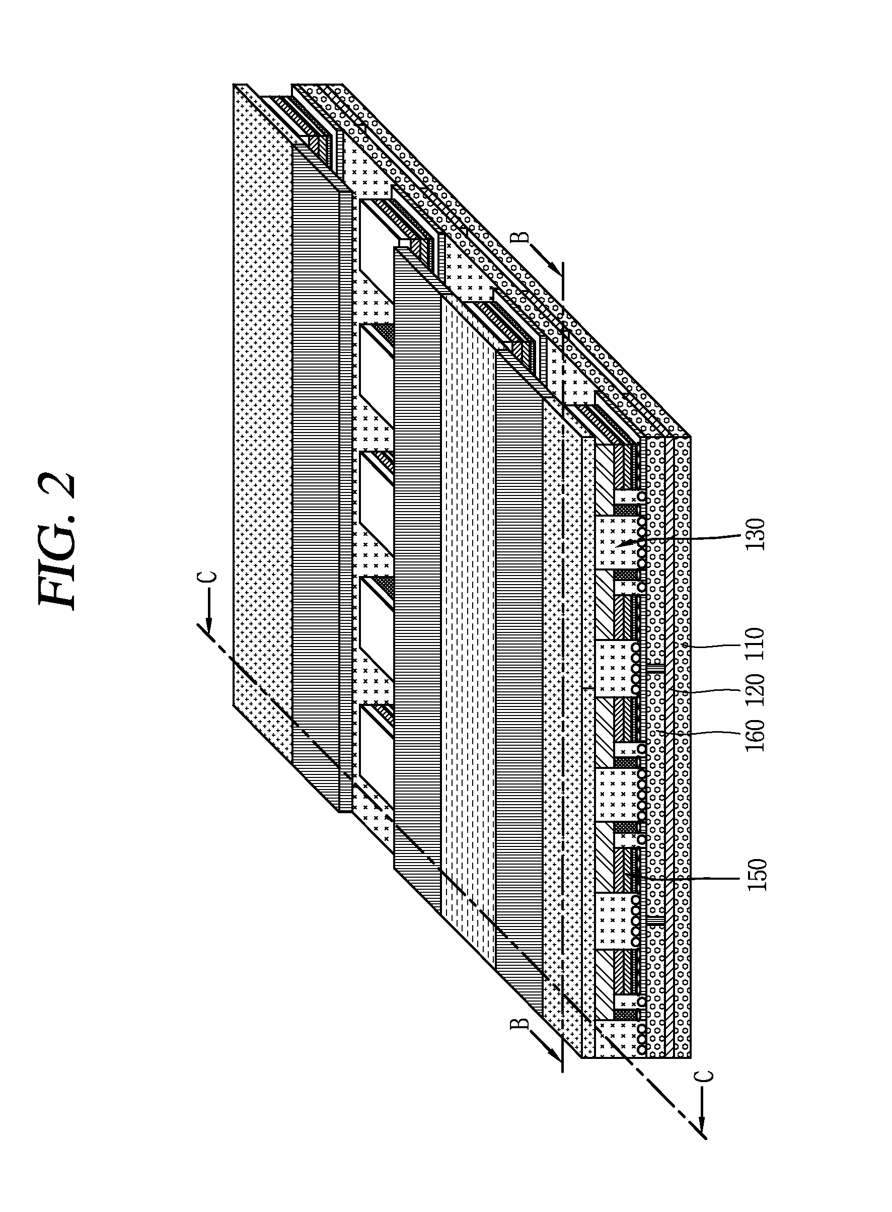
[0032]Hereinafter, the embodiments disclosed herein will be described in detail with reference to the accompanying drawings, and the same or similar elements are designated with the same numeral references regardless of the numerals in the drawings and their redundant description will be omitted. A suffix “module” or “unit” used for constituent elements disclosed in the following description is merely intended for easy description of the specification, and the suffix itself does not give any special meaning or function. Also, the accompanying drawings are merely illustrated to easily explain the concept of the invention, and therefore, they should not be construed to limit the technological concept disclosed herein by the accompanying drawings. Furthermore, when an element such as a layer, region or substrate is referred to as being “on” another element, it can be directly on the another element or an intermediate element may also be interposed therebetween.

[0033]A display device di...


PUM


Abstract

A method of transferring a semiconductor light emitting device, and which includes positioning a transfer head having a head electrode facing a semiconductor light emitting device having an undoped semiconductor layer, the semiconductor light emitting device arranged on a carrier substrate; moving the head electrode of the transfer head close to the undoped semiconductor layer of the semiconductor light emitting device; applying a voltage to the head electrode to provide an attachment force to the undoped semiconductor layer by an electrostatic force; and picking-up the semiconductor light emitting device and transferring the semiconductor light emitting device to base substrate.

Description

CROSS-REFERENCE TO RELATED APPLICATION[0001]Pursuant to 35 U.S.C. §119(a), this application claims the benefit of earlier filing date and right of priority to Korean Application No. 10-2015-0049187, filed on Apr. 7, 2015, the contents of which is incorporated by reference herein in its entirety.BACKGROUND OF THE INVENTION[0002]1. Field of the Invention[0003]The present invention relates to a display device using a semiconductor light emitting device and a method of manufacturing the same, and more particularly, a semiconductor light emitting device, a transfer head of a semiconductor light emitting device, and a method of transferring a semiconductor light emitting device.[0004]2. Background of the Invention[0005]In recent years, display devices having excellent characteristics such as low profile, flexibility and the like have been developed in the display technical field. On the contrary, currently commercialized main displays are represented by liquid crystal displays (LCDs) and ...

Claims


Application Information

Patent Timeline
Patent Type & Authority Applications(United States)
IPC IPC(8): H01L21/683H02N13/00H01L25/075H01L33/62H01L33/24H01L33/38
CPCH01L21/6833H01L33/24H01L33/38H01L2933/0033H01L33/62H02N13/00H01L25/0753H01L33/00H01L33/36H01L21/6831H01L33/0095H01L2224/95
Inventor CHANG, YOUNGHAKJEON, JINA
Owner LG ELECTRONICS INC
Why Eureka
Try Eureka