Solar cell and method of manufacturing the same

US20160336468A1Active Publication Date: 2016-11-17SHANGRAO JINKO SOLAR TECH DEV CO LTD

Image

  • Solar cell and method of manufacturing the same
  • Solar cell and method of manufacturing the same
  • Solar cell and method of manufacturing the same

Examples


Embodiment Construction

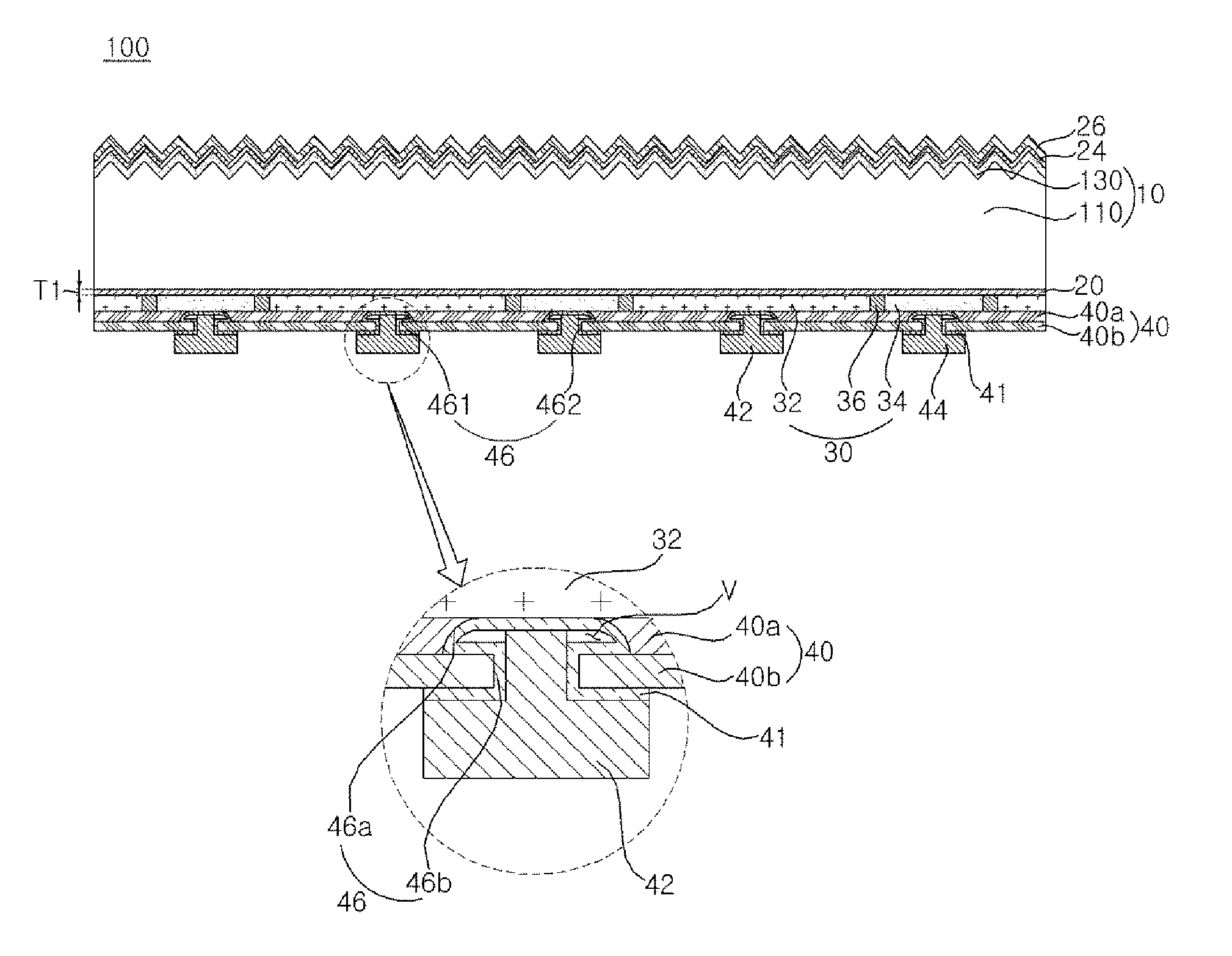
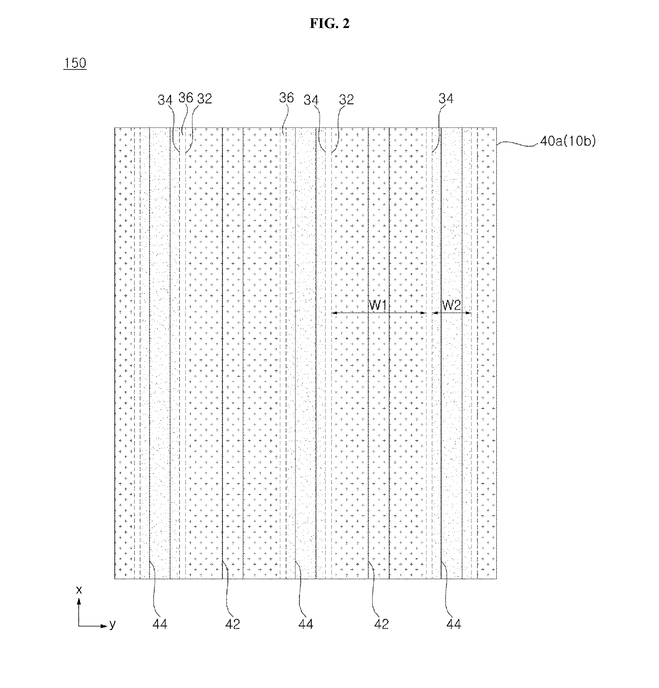
[0021]Reference will now be made in detail to the embodiments of the present invention, examples of which are illustrated in the accompanying drawings. However, it will be understood that the present invention should not be limited to the embodiments and may be modified in various ways.

[0022]In the drawings, to clearly and briefly explain the embodiments of the present invention, illustration of elements having no connection with the description is omitted, and the same or extremely similar elements are designated by the same reference numerals throughout the specification. In addition, in the drawings, for more clear explanation, the dimensions of elements, such as thickness, width, and the like, are exaggerated or reduced, and thus the thickness, width, and the like of the embodiments of the present invention are not limited to the illustration of the drawings.

[0023]In the specification, when an element is referred to as “including” another element, the element should not be under...


PUM


Abstract

Disclosed is a solar cell including a semiconductor substrate, a conductive area including a first conductive area and a second conductive area formed on one surface of the semiconductor substrate, a passivation film formed on the conductive area, the passivation film having a contact hole, a protective film formed on the conductive area inside the contact hole, the protective film being formed on at least one of at least a portion of an inner side surface of the contact hole and the passivation film, and an electrode electrically connected to the conductive area through the contact hole with the protective film interposed therebetween.

Description

CROSS-REFERENCE TO RELATED APPLICATION[0001]This application claims the priority benefit of Korean Patent Application No. 10-2015-0066630, filed on May 13, 2015 and Korean Patent Application No. 10-2016-0041767 filed on Apr. 5, 2016 in the Korean Intellectual Property Office, the disclosures of which are incorporated herein by reference.BACKGROUND OF THE INVENTION[0002]1. Field of the Invention[0003]Embodiments of the present invention relate to a solar cell and a method of manufacturing the same, and more particularly to a back contact solar cell and a method of manufacturing the same.[0004]2. Description of the Related Art[0005]Recently, due to depletion of existing energy resources, such as oil and coal, interest in alternative sources of energy to replace the existing energy resources is increasing. Most of all, solar cells are popular next generation cells to convert sunlight into electrical energy.[0006]Solar cells may be manufactured by forming various layers and electrodes b...

Claims


Application Information

Patent Timeline
17 Nov 2016
Publication
US20160336468A1
IPC
H01L31/049; H01L31/18; H01L31/0224; H01L31/0236; H01L31/02; H01L31/0216
CPC
H01L31/049; H01L31/02008; H01L31/1868; H01L31/022441; H01L31/02366; H01L31/02167; H01L31/02168; H01L31/022425
Inventors
CHUNG, INDO; YANG, JUHONG