

A pixel structure and a preparation method thereof, a pixel display method and an array substrate
- Summary
- Abstract
- Description
- Claims
- Application Information
AI Technical Summary
Benefits of technology
Problems solved by technology
Method used
Image

Examples
embodiment i
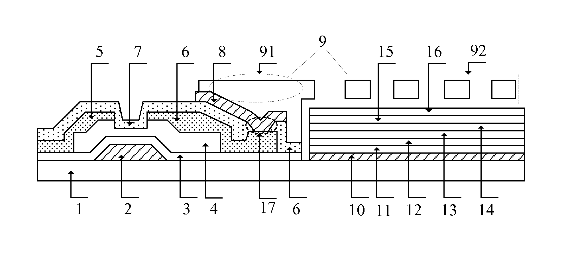
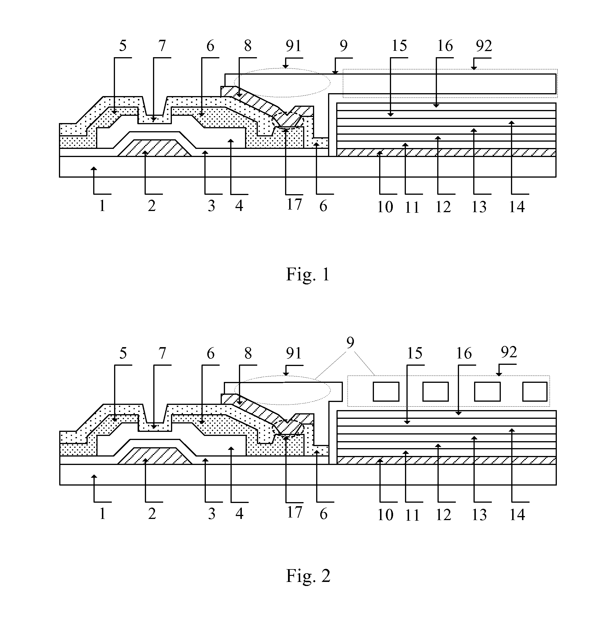
[0056]Referring to FIG. 1, the pixel structure comprises a thin film transistor
[0057](TFT), a quantum dot light emitting diode (QLED) device spaced apart from the TFT, the thin film transistor comprises a gate electrode 2, a gate insulating layer 3, an active layer 4, a source electrode 5, a drain electrode 6 and an insulating layer 7 formed on a substrate 1 successively, a first via hole 17 is formed on the insulating layer 7, the first via hole 17 corresponds to at least part of the drain electrode 6 of the TFT. In the embodiment of the present disclosure, the TFT is a bottom gate type structure, the insulating layer 7 is a passivation layer or a combination of a passivation layer and a planarization layer.
[0058]The pixel structure further comprises a first conductive structure 8 formed over the insulating layer 7, the first conductive structure 8 is electrically connected with the drain electrode 6, the first conductive structure 8 is electrically connected with the drain electro...
embodiment ii
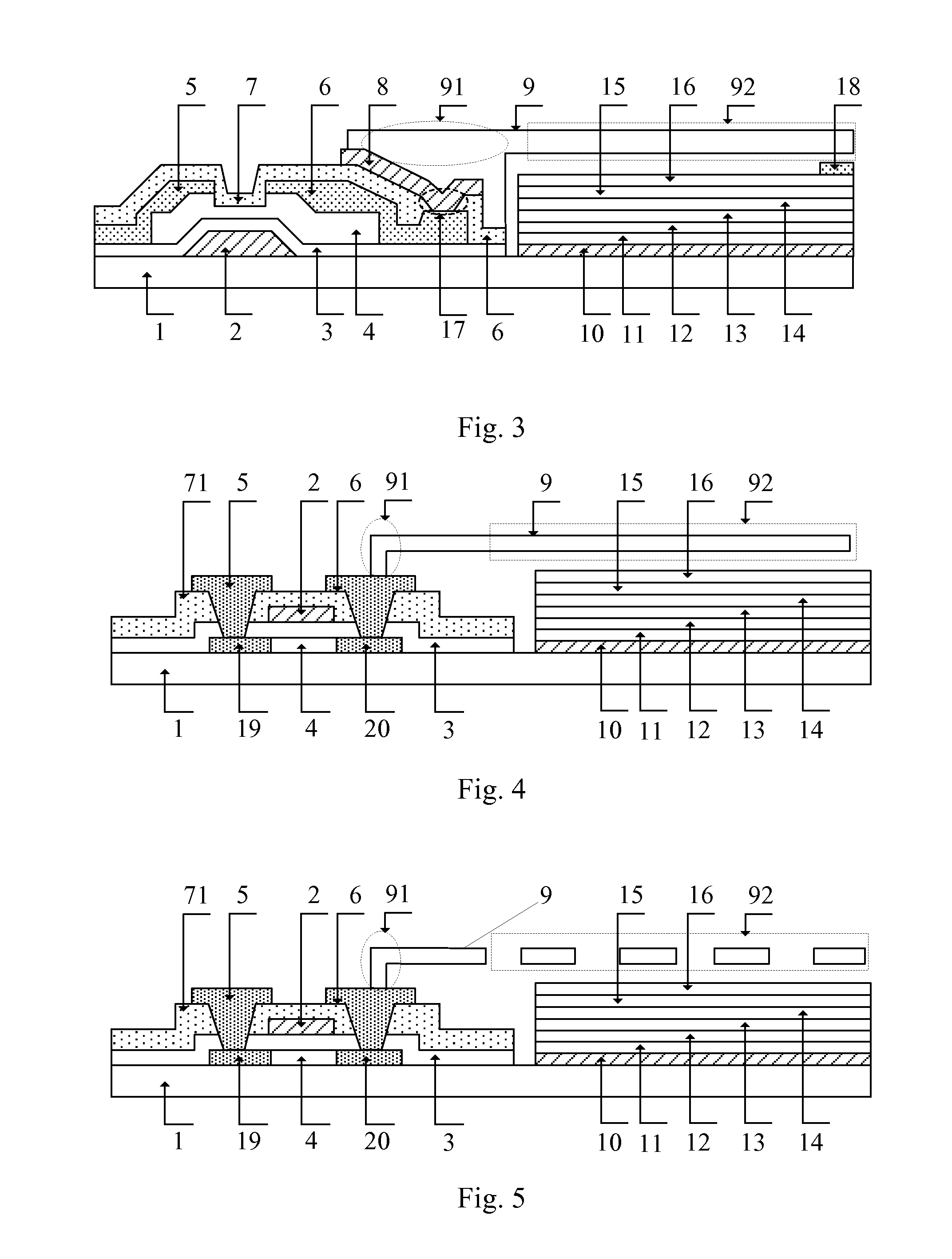
[0065]Referring to FIG. 4, another pixel structure is provide, the pixel structure comprising a thin film transistor (TFT), a quantum dot light emitting diode (QLED) device spaced apart from the TFT, the thin film transistor comprises an ohmic contact layer, an active layer 4, a gate insulating layer 3, a gate electrode 2, a passivation layer 71 and a source-drain electrode metal layer formed on a substrate 1 successively; The ohmic contact layer comprises a first electrode 19 and a second electrode 20, the source-drain metal layer comprises a source electrode 5 and a drain electrode 6. The TFT is a top gate type structure, compared with the above bottom gate type TFT, this embodiment is not a simple transformation and replacement from the bottom gate type to the top gate type, this optional embodiment uses a TFT of the top gate type structure which enables the connecting portion 91 to contact with the drain electrode 6 directly when fabricating the MEMS switch, which simplifies the...
embodiment iii
[0071]The embodiment of the present disclosure provides an array substrate comprising a plurality of pixel units arranged in an array, each pixel unit adopts a pixel structure provided by the above embodiment.
[0072]Optionally, for the consideration of simplifying the fabricating process and saving the working procedure, the QLED of each column of pixel can be made as a whole, i.e., according to the corresponding arrangement manner of the R, G, B color resistances as shown in FIG. 7.
[0073]The beneficial effect of the embodiment of the present disclosure is as follows: a MEMS switch is added in the pixel structure, the MEMS switch is electrically connected with the first conductive structure; when the display device works, the QLED device emits light constantly, the TFT controls the light emission amount of the outgoing light of the QLED device by controlling the switching amplitude of the MEMS switch, so as to avoid frequent flicker of the QLED device and increase the life time of th...
PUM
 Abstract
Description
Claims
Application Information