Chip package
a chip and chip technology, applied in the field of electronic chip packaging, can solve the problems of affecting the use of single layer structures,
- Summary
- Abstract
- Description
- Claims
- Application Information
AI Technical Summary
Benefits of technology
Problems solved by technology
Method used
Image

Examples
Embodiment Construction
[0101]In the description hereinbelow, support structures consisting of metal vias in a dielectric matrix, particularly, copper via posts in a polymer matrix, such as polyimide, epoxy or BT (Bismaleimide / Triazine), Polyphenylene Ether (PPE), Polyphenylene Oxide (PPO) or their blends, reinforced with glass fibers are considered.
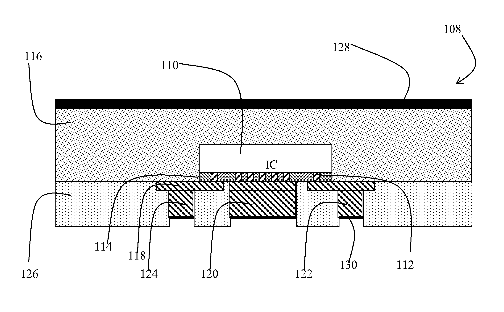
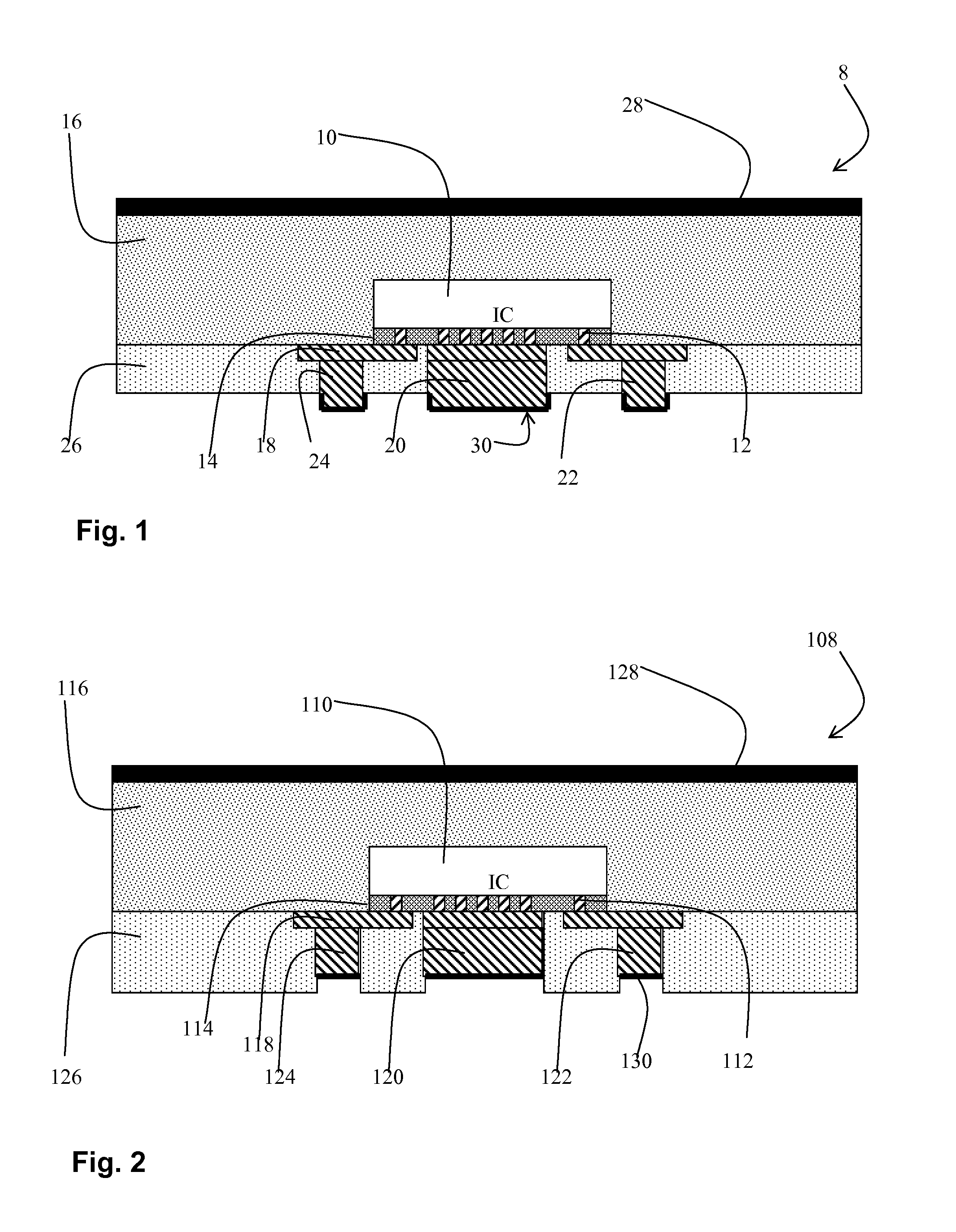
[0102]With reference to FIG. 1, a simplified section through an electronic chip package 8 in accordance with one embodiment that enables coupling a chip 10 to a substrate by a Land Grid Array (LGA) 20, 22, 24 is shown.
[0103]The electronic chip package 8 consists of a die or chip 10 with aluminum pillars 12 in a passivation layer 14 comprises either PI or SiN.
[0104]The chip 10 with aluminum pillars 12 in a passivation layer 14 is encapsulated by laminating with a first dielectric material 16 having a polymer matrix such as polyimide, epoxy or BT (Bismaleimide / Triazine), Polyphenylene Ether (PPE), Polyphenylene Oxide (PPO) or their blends, either provided as a fi...
PUM
 Abstract
Description
Claims
Application Information
 - R&D Engineer
- R&D Manager
- IP Professional
- Industry Leading Data Capabilities
- Powerful AI technology
- Patent DNA Extraction
Browse by: Latest US Patents, China's latest patents, Technical Efficacy Thesaurus, Application Domain, Technology Topic.
© 2024 PatSnap. All rights reserved.Legal|Privacy policy|Modern Slavery Act Transparency Statement|Sitemap