
Integrated current sensor system and method for producing an integrated current sensor system

a current sensor and sensor technology, applied in the direction of voltage/current isolation, measurement devices, instruments, etc., can solve the problems of limited sensitivity of current sensor implementations, high material and production process costs, etc., and achieve the effect of improving sensitivity and reducing production effor

Active Publication Date: 2017-01-12
AMS AG
View PDF5 Cites 4 Cited by
  • Summary
  • Abstract
  • Description
  • Claims
  • Application Information

AI Technical Summary

Benefits of technology

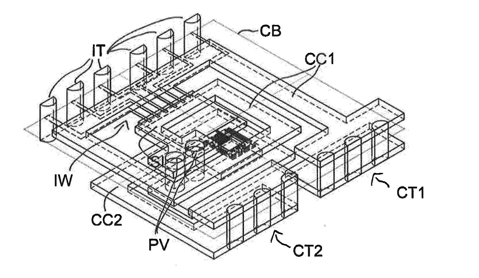
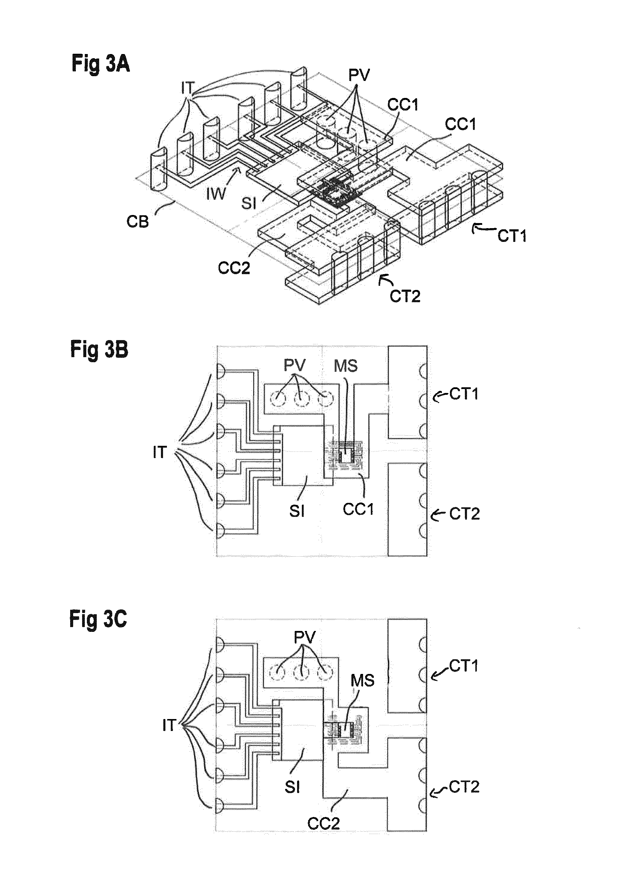
The present patent provides an improved design for integrated current sensor systems that increases sensitivity and reduces production effort. The improvement involves placing current conductors on both sides of the sensing area, i.e. on both sides of a magnetic field sensor. This double-sided placement creates a higher magnetic field, resulting in a stronger signal from the sensor. The magnetic field sensor and interface are embedded in a printed circuit board, with conductive vias connecting the current conductors. The resulting structure has the same form factor as a standard package and can be easily soldered. The current conductors are designed in a coil-like structure to increase the magnetic field intensity and field strength. Overall, this innovation increases the sensitivity of the integrated current sensor system.

Problems solved by technology

However, such implementations result in high costs with regard to the material and with regard to the production process.
Additionally, the sensitivity of such current sensor implementations is limited due to inductive effects.

Method used


Image

  • Integrated current sensor system and method for producing an integrated current sensor system
  • Integrated current sensor system and method for producing an integrated current sensor system
  • Integrated current sensor system and method for producing an integrated current sensor system

Examples


Embodiment Construction

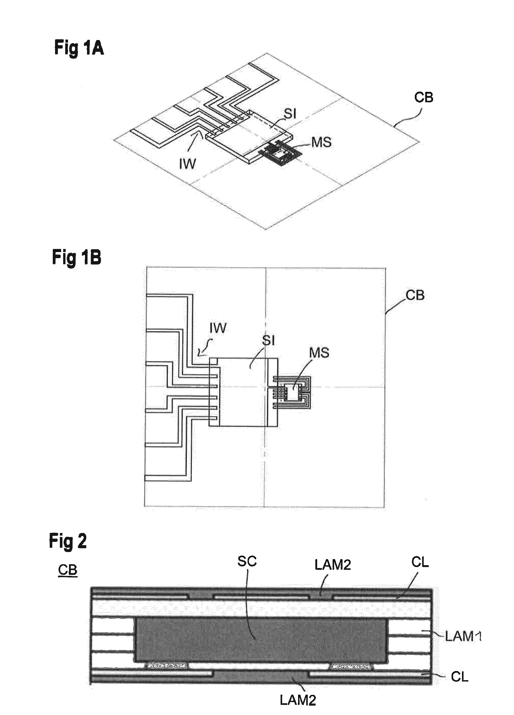
[0030]FIGS. 1A and 1B show a printed circuit board, PCB, CB in detail, respectively an intermediate production step of an integrated current sensor system according to the improved concept. On the circuit board CB a magnetic field sensor MS and a corresponding sensor interface SI connected to the magnetic field sensor MS are integrated. Respective interface wires IW for connecting the sensor interface SI are further integrated on the circuit board CB.

[0031]In the embodiment shown, the magnetic field sensor MS and the sensor interface SI are provided as two separate dies. However, in alternative implementations the sensor interface SI and the magnetic field sensor MS may be provided as a single die. The magnetic field sensor may be a Hall sensor, which preferably is fabricated in GaAs technology, allowing a high sensitivity of the Hall sensor. The sensor interface SI may be implemented as an application-specific integrated circuit, ASIC, which may be made of silicon. The magnetic fie...


PUM


Abstract

An integrated current sensor system has a printed circuit board with a magnetic field sensor with a sensor interface. The printed circuit board has a first side on which, isolated from the printed circuit board, a first current conductor is arranged with a longitudinal edge of a portion of the first current conductor being proximate to a sensitive area of sensor. The circuit board has a second side on which a second current conductor is, isolated from the printed circuit board, arranged, wherein a longitudinal edge of a portion of the second current conductor is arranged proximate to the sensitive area. The first and the second current conductor are electrically connected with at least one conductive via.

Description

[0001]The present disclosure relates to an integrated current sensor system, in particular for galvanically isolated current sensing, and to a method for producing such current sensor systems.BACKGROUND OF THE INVENTION[0002]Current sensors are used for a variety of applications, for example current limitation, overcurrent protection or simply for monitoring the intensity of a current. For such applications magnetic field sensors like Hall sensors are widely used. Such magnetic field sensors sense the magnetic field generated by a current flowing through a current conductor and provide a measurement signal proportional to the intensity of the current. As the magnetic field decreases with increasing distance between the magnetic field sensor and the current conductor, it is tried to bring the magnetic field sensor close to the conductor carrying the current to be measured in order to have a sufficiently strong magnetic field.[0003]In various implementations, leadframes of a sensor pa...

Claims


Application Information

Patent Timeline
IPC IPC(8): G01R15/20G01R33/00
CPCG01R33/0052G01R15/202G01R15/207
Inventor ETSCHMAIER, HARALD
Owner AMS AG
Learn More