Support for long channel length nanowire transistors

Inactive Publication Date: 2017-01-19
IBM CORP
View PDF7 Cites 0 Cited by
  • Summary
  • Abstract
  • Description
  • Claims
  • Application Information

AI Technical Summary

Benefits of technology

The patent describes a device called a nanowire that connects a source and a drain on a substrate. The nanowire is supported and prevented from sagging by an anchor pad, which helps to maintain its stability. The technical effect of this invention is a more reliable and efficient connection between the source and drain, resulting in improved performance of the device.

Problems solved by technology

Nanowire FETs may be subject to physical degradation due to mechanical changes, such as sagging.
Specifically, in gate all-around structures, long channel devices include long unsupported spans that tend to sag or otherwise deflect either immediately or over time.
This deflection can cause the nanowire to touch the substrate or other components, resulting in an undesired result or short.
Long lengths of nanowire can cause mechanical sagging and therefore a lack of structural integrity.

Method used


Image

  • Support for long channel length nanowire transistors
  • Support for long channel length nanowire transistors
  • Support for long channel length nanowire transistors

Examples


Embodiment Construction

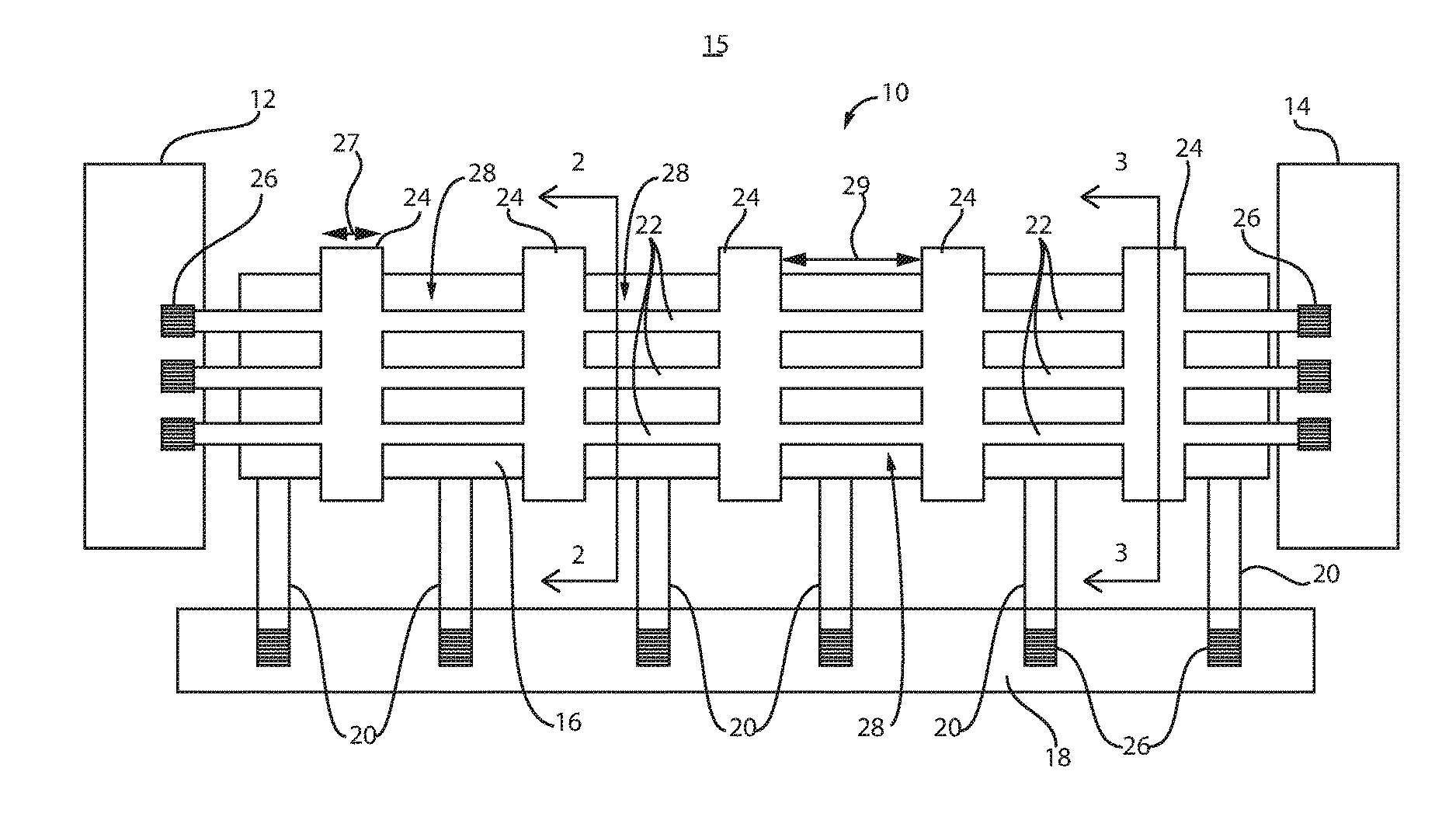
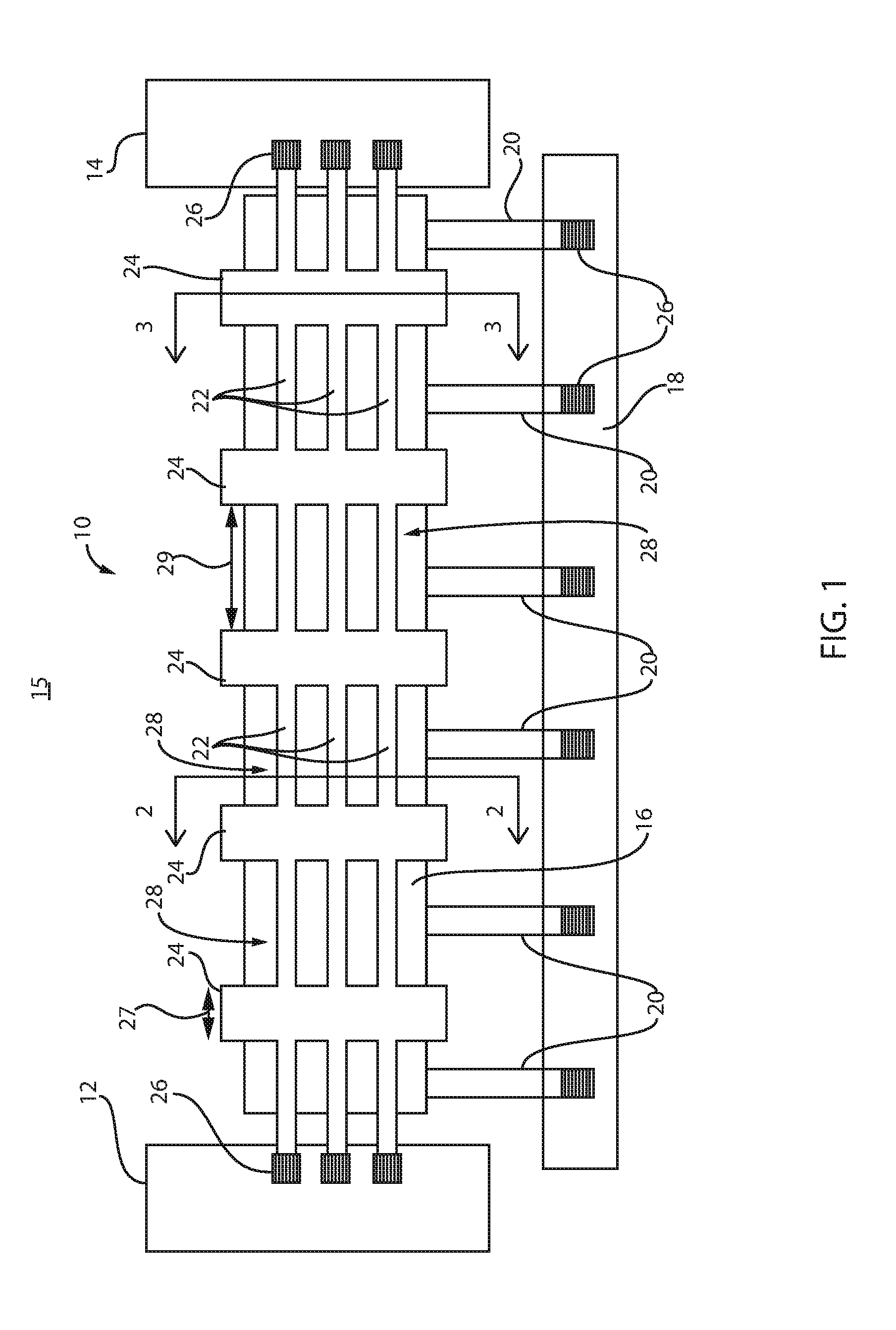
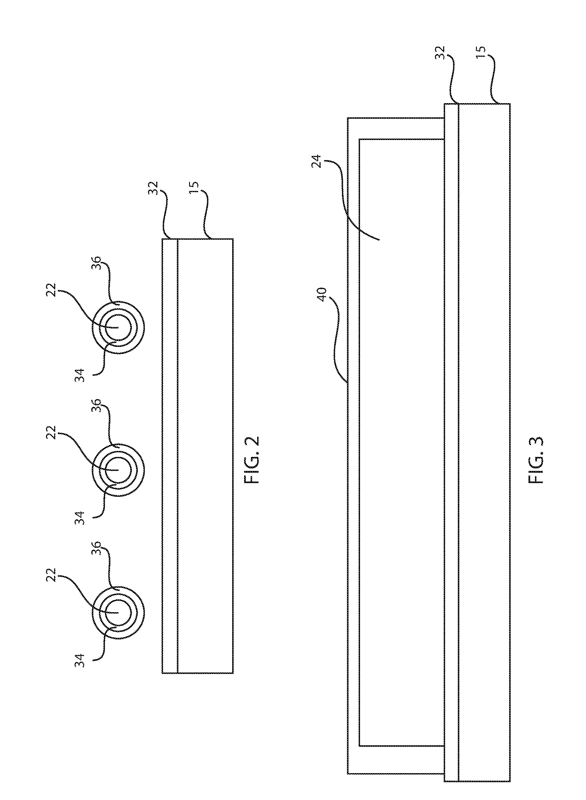
[0014]In accordance with the present principles, nanowires and methods for formation of nanowires are provided. The nanowires include anchor pads disposed between sections or segments of nanowires to prevent nanowire sagging. The anchor pads may vary in size and number, and may be placed at different distances along the nanowire(s). The anchor pads are preferably integrally formed with the nanowires, and preferably include the same materials and are formed in a same formation process. True nanowire current can be computed by subtracting out the influences of the anchor pads based pad width(s) of the anchor pads to extract current as though the anchor pads were not present.

[0015]The nanowires described herein include gate all-around nanowires. It should be understood that the nanowires may have other structures and configurations. For example, the nanowires may be included as a device channel for a nanowire transistor but may also be employed as conductive lines. In addition, the nan...


PUM


Abstract

A nanowire device includes a first component formed on a substrate and a second component disposed apart from the first component on the substrate. A nanowire is configured to connect the first component to the second component. An anchor pad is formed along a span of the nanowire and configured to support the nanowire along the span to prevent sagging.

Description

BACKGROUND[0001]Technical Field[0002]The present invention relates to semiconductor devices, and more particularly to nanowire devices having a long channel length with reduced sagging.[0003]Description of the Related Art[0004]Nanowire field effect transistors (FETs) may be employed for a number of applications. Nanowire FETs may be subject to physical degradation due to mechanical changes, such as sagging. Specifically, in gate all-around structures, long channel devices include long unsupported spans that tend to sag or otherwise deflect either immediately or over time. This deflection can cause the nanowire to touch the substrate or other components, resulting in an undesired result or short. Long lengths of nanowire can cause mechanical sagging and therefore a lack of structural integrity.SUMMARY[0005]A nanowire device includes a first component formed on a substrate and a second component disposed apart from the first component on the substrate. A nanowire is configured to conn...

Claims


Application Information

Patent Timeline
IPC IPC(8): H01L29/06H01L29/423H01L29/66
CPCH01L29/0673H01L29/42392H01L29/66477B82Y10/00H01L29/42356H01L29/4238H01L29/0649H01L29/775H01L29/78696H01L29/0657H01L23/562H01L21/02603H01L29/66742H01L29/0669H01L29/66439H01L21/02403H01L29/78603H01L29/78618
Inventor BALAKRISHNAN, KARTHIKLAUER, ISAACYAMASHITA, TENKOSLEIGHT, JEFFREY W.
Owner IBM CORP
Why Eureka
Try Eureka