Semi-close loop DC offset compensation technique

a compensation technique and semi-close loop technology, applied in the field of semi-close loop dc offset compensation technique, can solve the problems of dc offset being undesirable, being exposed to interference from other transmitters, microwave ovens, other appliances, etc., and achieve accurate calibration, time saving, and accuracy.

Inactive Publication Date: 2017-02-09
GAINSPAN
View PDF2 Cites 0 Cited by
  • Summary
  • Abstract
  • Description
  • Claims
  • Application Information

AI Technical Summary

Benefits of technology

[0011]This new method avoids the problem brought on by uncertainty, while saving time. Embodiments of the invention are directed to a procedure for accurately calibrating the DC Offset in the receiver chain at a speed similar to open loop solutions, but with accuracy similar to close loop solutions, and which can be done in the factory or in the final product in the field. The calibration process begins by determining the step size and then determining the DC offset compensation using the determined step size. Due to the nature of the analog blocks, the DAC step size is different for each and every chip and this also varies with temperature. Calculating the DAC step size for every chip brings accuracy to the calibrations. With this in hand, the calculation for calibrated DAC values is straight forward resulting in significant amount of time reduction. Further, identifying the DAC step size for each individual chip makes it more a robust calibration.

Problems solved by technology

DC offset is usually undesirable because it causes saturation or change in the operating point of an amplifier in the wireless device.
When a receiver (or wireless chipset) is integrated in a final product and connected to an antenna, it is exposed to all kind of interferences from other transmitters, microwave ovens, other appliances, and the like.
Although a manufacturer of a wireless chipset can calibrate the chipset itself, the final product may still suffer from DC offset because the impedance of the antenna is different for each product.
In addition, DC offset can also be affected whenever there is saturation caused by interferences or when there is interference at very low frequency offsets from LO frequencies.
Depending on the LO leakage power level, all receivers suffer from DC offset caused by self-mixing of the LO with its leakage.
It is impossible and impractical to predict the impedance in the final products; thus, it is impossible to predict the DC offset in the final products.
This uncertainty causes a problem in determining DC offset cancellation.
This approach yields more reliable results but is very time consuming as it has to go through many possible values and at least one measurement of DC at each setting.
However, the precise DAC step size has to be measured on some a test setup in the factor, and, therefore, cannot be obtained once the products are off the product line.
This requirement of precise measurement also increases the total cost of the products.

Method used


Image

  • Semi-close loop DC offset compensation technique
  • Semi-close loop DC offset compensation technique
  • Semi-close loop DC offset compensation technique

Examples


Embodiment Construction

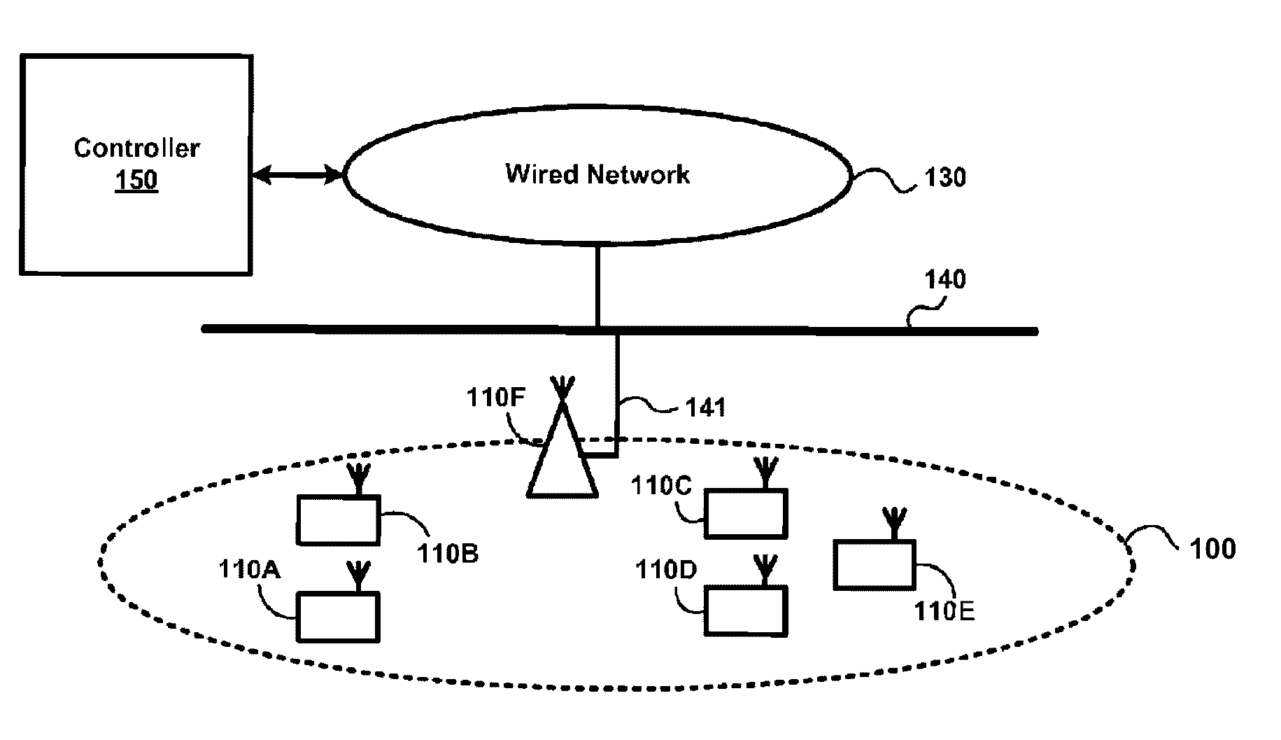
[0021]FIG. 1 illustrates an exemplary network including both wired and wireless components. It will be appreciated that the network shown in FIG. 1 and described herein is exemplary and fewer or additional components may be included in the network and other variations may be made to the exemplary network are contemplated. In addition, although certain features of the network are described with reference to a network consistent with the IEEE 802.11 standards; it will be appreciated that the invention may be implemented in networks operating with other wireless network standards, such as, for example, HIPERLAN, IEEE 802.16, Bluetooth, cellular technologies, such as CDMA, WCDMA, LTE, etc., and others, or other non-standards-based wireless networks.

[0022]The network 100 illustrated in FIG. 1A includes clients 110A-110E, access point (AP) 110F, wired network 130, wired network backbone 140 and wireless network manager 150. Client 110 represents a basic service set (BSS) consistent with t...


PUM


Abstract

Systems and methods for calibrating DC offset of wireless device are disclosed. The calibration process includes determining the DC offset based on the step size determined for each particular wireless chipset or wireless device, which may be determined in the factory or in the field. The DAC compensation corresponding to the DC offset may then be applied to the baseband of the receive chain of the chipset.

Description

BACKGROUND[0001]1. Field[0002]The present disclosure relates generally to wireless devices, and, more specifically, to systems and methods for a semi-close loop DC offset compensation technique.[0003]2. Related Art[0004]A wireless network generally includes two or more wireless devices that communicate with each other over a wireless medium. One example of a wireless network is a wireless local area network (WLAN) designed to operate according to IEEE 802.11 standards.[0005]DC offset is usually undesirable because it causes saturation or change in the operating point of an amplifier in the wireless device. When a receiver (or wireless chipset) is integrated in a final product and connected to an antenna, it is exposed to all kind of interferences from other transmitters, microwave ovens, other appliances, and the like. DC Offset is particularly sensitive to input impedance. Although a manufacturer of a wireless chipset can calibrate the chipset itself, the final product may still su...

Claims


Application Information

Patent Timeline
Patent Type & Authority Applications(United States)
IPC IPC(8): H04B1/10H04B17/21
CPCH04B17/21H04B1/1027H04B17/104
Inventor VAISHNAV, RAVI KUMAR
Owner GAINSPAN
Why Eureka
Try Eureka