Display device and method for driving same

a display device and a technology for driving the same, applied in the field of display devices, can solve the problems of difficulty in achieving size increase and definition improvement, luminance non-uniformity on the display screen, etc., and achieve the effect of reducing the cost of the display device and simple configuration

Active Publication Date: 2017-06-08
SHARP KK
View PDF5 Cites 17 Cited by
  • Summary
  • Abstract
  • Description
  • Claims
  • Application Information

AI Technical Summary

Benefits of technology

[0105]According to the first aspect of the present invention, in the drive control unit there is provided the matching determination circuit that determines whether the number of clock pulses of a first clock signal group which controls the operation of the write control line drive circuit matches a measurement target address value indicating a measurement target row. Then, if the number of clock pulses of a first clock signal group matches the measurement target address value indicating a measurement target row, the drive control unit stops clock operation performed by the first clock signal group for a predetermined period (current measurement period) from a time point that is one clock period after a time point where they match each other. In addition, at the start time point and end time point of the current measurement period, the drive control unit changes only a potential of one of clock signals that is provided to a first unit circuit corresponding to the measurement target row, the clock signals being included in the first clock signal group. By this, a write control line of the measurement target row goes into a selected state during periods immediately before and immediately after the current measurement period. In addition, the monitoring control line drive circuit is configured to bring a monitoring control line corresponding to a second unit circuit being in an active state into a selected state when a monitoring enabling signal is active. Here, the drive control unit stops clock operation performed by a second clock signal group for a predetermined period (current measurement period) from a time point that is one clock period after a time point where the number of clock pulses of the first clock signal group matches the measurement target address value indicating a measurement target row. By this, in each frame period, a monitoring control line of a measurement target row goes into a selected state during the current measurement period, and all monitoring control lines are maintained in a non-selected state during other periods. By driving the write control lines and the monitoring control lines in the above-described manner, in each frame period, drive current measurement for detecting characteristics of drive transistors is performed. Then, correction data is obtained based on the measured values of drive currents, and grayscale data is corrected based on the correction data. As a result, variations in the characteristics of the drive transistors are compensated for. Here, the shift registers in the gate driver circuits (the write control line drive circuit and the monitoring control line drive circuit) that implement the above-described operation are formed using transistors of only one of an N-channel type and a P-channel type. By the above, it becomes possible to compensate for variations in the characteristics of drive transistors in a display device that includes current-driven self light-emitting type display elements and that adopts gate driver circuits formed of single-channel transistors. Meanwhile, the gate driver circuits that perform complex operation to enable drive current measurement such as that described above are generally implemented by CMOS logic circuits. Hence, according to conventional art, when transistors other than polysilicon TFTs are adopted as transistors composing the gate driver circuits, the gate driver circuits that perform complex operation cannot be formed on a glass substrate. Therefore, the gate driver circuits need to be mounted on a glass substrate in IC chip form. Regarding this point, according to the first aspect of the present invention, complex operation is implemented by gate driver circuits formed using single-channel transistors. Hence, the gate driver circuits can be formed on a glass substrate without being formed in IC form. As a result, a reduction in the cost of a display device is achieved.
[0106]According to the second aspect of the present invention, the monitoring control line drive circuit capable of bringing a monitoring control line into a selected state only during the current measurement period is implemented by a relatively simple configuration.
[0107]According to the third aspect of the present invention, it becomes possible to securely increase the level of a voltage provided to the control terminal of the output control transistor to a level sufficient to bring the monitoring control line into a selected state.
[0108]According to the fourth aspect of the present invention, it becomes possible for the correction data calculation and storage unit to identify whether a measured value of a drive current provided from the current measurement circuit is a value based on the first grayscale or a value based on the second grayscale. Hence, calculation of correction data is securely performed based on two types of drive currents.
[0109]According to the fifth aspect of the present invention, a grayscale identification counter does not need to be provided for each row, and only one grayscale identification counter needs to be provided for the entire device.
[0110]According to the sixth aspect of the present invention, the same effects as those of the first aspect of the present invention can be obtained with a display device including a matching determination circuit including a plurality of exclusive-OR circuits, a plurality of NOT circuits, and an AND circuit.

Problems solved by technology

An organic EL display device adopting the passive matrix system is simple in structure, but is difficult to achieve size increase and definition improvement.
As a result, luminance nonuniformity occurs on a display screen.

Method used


Image

  • Display device and method for driving same
  • Display device and method for driving same
  • Display device and method for driving same

Examples


Embodiment Construction

[0155]An embodiment of the present invention will be described below with reference to the accompanying drawings. Note that for each transistor, a gate terminal corresponds to a control terminal, a drain terminal corresponds to a first conduction terminal, and a source terminal corresponds to a second conduction terminal.

[0156]

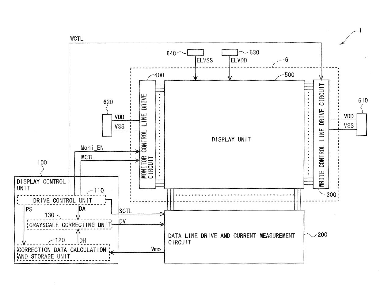
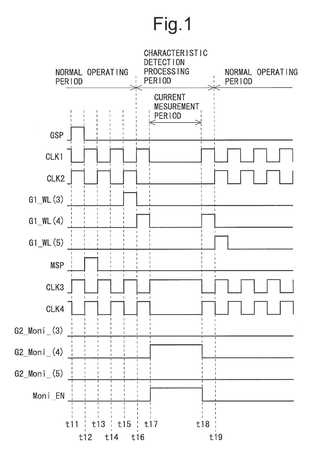
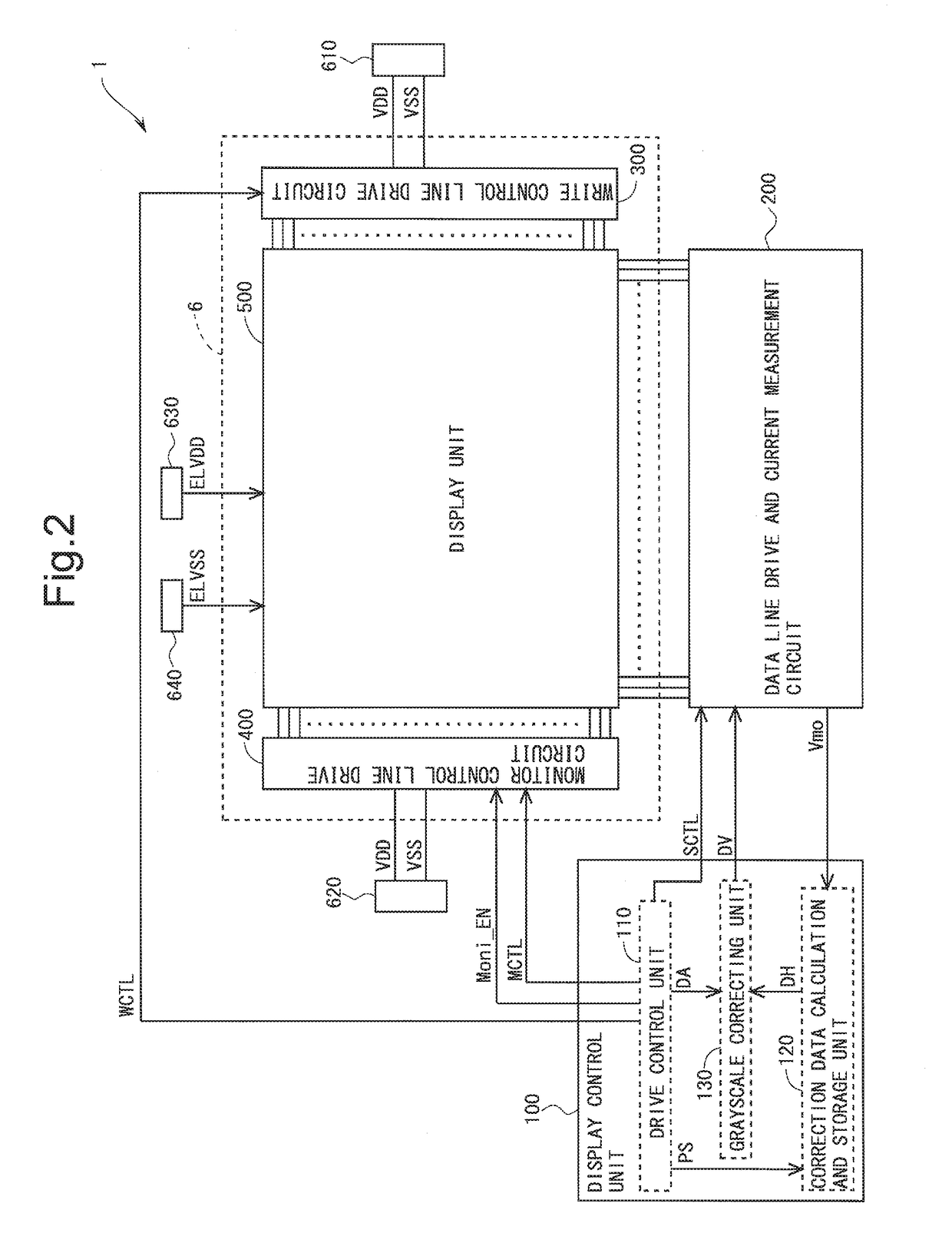
[0157]FIG. 2 is a block diagram showing an overall configuration of an active matrix-type organic EL display device 1 according to one embodiment of the present invention. The organic EL display device 1 includes a display control circuit 100, a data line drive and current measurement circuit 200, a write control line drive circuit 300, a monitoring control line drive circuit 400, and a display unit 500. As shown in FIG. 3, the data line drive and current measurement circuit 200 includes a portion that functions as a data line drive circuit 210 and a portion that functions as a current measurement circuit 220. Note that in the present embodiment, the write con...


PUM


Abstract

When a clock signal pulse number and a compensation-target-line address indicating a compensation-target row match, the following control is carried out with a time point being a starting point of a current measurement period, the time point being one horizontal scanning period after a time point of the match. At a current measurement period starting point and ending point, only the potential of the one of the clock signals applied to a unit circuit corresponding to the compensation-target row is changed. Throughout the current measurement period, the clock operation of the clock signals is stopped. A monitor enable signal, that is applied to a control terminal of an output control transistor for controlling active signal output to a monitor control line, is only set to a high level during the current measurement period.

Description

TECHNICAL FIELD[0001]The present invention relates to a display device and more particularly to a display device including self light-emitting type display elements which are driven by a current, such as an organic EL display device, and a method for driving the display device.BACKGROUND ART[0002]Conventionally, as display elements included in a display device, there are an electro-optical element whose luminance is controlled by a voltage applied thereto, and an electro-optical element whose luminance is controlled by a current flowing therethrough. A representative example of the electro-optical element whose luminance is controlled by a voltage applied thereto includes a liquid crystal display element. On the other hand, a representative example of the electro-optical element whose luminance is controlled by a current flowing therethrough includes an organic EL (Electro Luminescence) element. The organic EL element is also called an OLED (Organic Light-Emitting Diode). An organic...

Claims


Application Information

Patent Timeline
Patent Type & Authority Applications(United States)
IPC IPC(8): G09G3/20G09G3/3258H01L51/50G09G3/3266H01L27/32G09G3/3291G09G3/3233
CPCG09G3/2018G09G3/3291G09G3/3258G09G3/3233G09G3/3266H01L27/3244G09G2300/0814H01L51/5036G09G2310/08G09G2320/0626G09G2320/0295G09G2310/0286G09G2310/0289H01L27/3211G09G2300/0819G09G2300/0842G09G2310/0262G09G2320/043G09G2320/045H10K50/125H10K59/12H10K59/35
Inventor OHARA, MASANORINOGUCHI, NOBORUKISHI, NORITAKA
Owner SHARP KK
Why Eureka
Try Eureka