Printed wiring board

a printing and wiring board technology, applied in the direction of printed circuits, printed circuit aspects, coupling device connections, etc., can solve the problems of thickness and size, difficulty in etc., and achieve the effect of reducing thickness and size of printed wiring boards and enhancing the engaging for

Active Publication Date: 2017-06-22
THE FUJIKURA CABLE WORKS LTD +1
View PDF0 Cites 6 Cited by
  • Summary
  • Abstract
  • Description
  • Claims
  • Application Information

AI Technical Summary

Benefits of technology

[0019]According to the present invention, the engageable part and the reinforcement layer(s) are disposed at appropriate locations and it is therefore possible to enhance the engaging force between the printed wiring board of a multilayer structure and a connector while achieving a reduced thickness and size of the printed wiring board of a multilayer structure.

Problems solved by technology

In a printed wiring board of a multilayer structure, however, it is difficult to enhance the engaging force between the printed wiring board and a connector while achieving a reduced thickness and size, which may be problematic.

Method used


Image

  • Printed wiring board
  • Printed wiring board
  • Printed wiring board

Examples


example 1

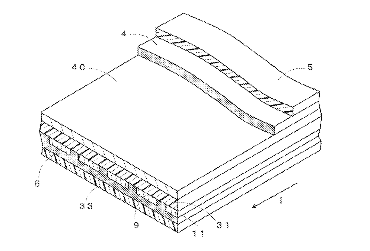
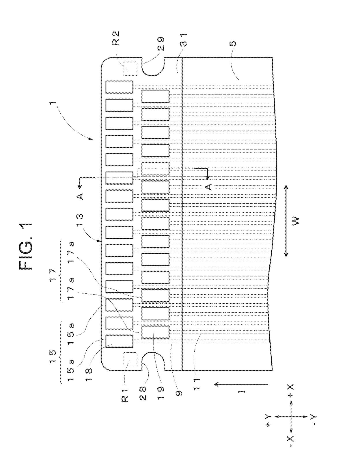
[0155]As Example 1, a printed wiring board 1 of a multilayer structure having the structure illustrated in FIGS. 1 to 4 was produced. The first substrate 31, second substrate 32, and third substrate 33 were produced through a scheme using a photolithography technique for the first wirings 9, second wirings 11, pads 15 and 17, and reinforcement layers R1 and R2.

[0156]Double-sided copper clad laminates were used as the first substrate 31, second substrate 32, and third substrate 33. Each double-sided copper clad laminate has a polyimide film of a thickness of 20 [μm] and copper foil layers formed on the polyimide film. The arrangement of the pads 15 and 17 is as illustrated in FIG. 1. Pitch of the pads 15 and 17 was 0.175 [mm] (0.35 [mm] in each array). The material of the pads 15 and 17, first wirings 9, second wirings 11, and reinforcement layers R1 and R2 was copper. The reinforcement layers R1 and R2 had a width of 0.5 [mm], length of 0.5 [mm], and thickness of 22.5 [μm] (copper: ...

example 2

[0163]As Example 2, the printed wiring board 1 was produced as in Example 1 except that the reinforcement layers R1 and R2 were formed integrally with some of the first wirings 9 and second wirings 11.

example 3

[0164]As Example 3, the printed wiring board 1 was produced as in Example 1 except that the reinforcement layers R1 and R2 were formed on the one main surface of the first substrate 31 and formed separately from the pads 15 and 17.


PUM


Abstract

A printed wiring board including: a first substrate on which a plurality of pads to be connected to a connector is arranged to form a front array and a rear array in two rows; a second substrate that is laminated on the first substrate and formed with first wirings connected to first pads of the front array and second wirings connected through vias to second pads of the rear array; engageable parts that are to be engaged with engagement parts of the connector; and one or more reinforcement layers that are provided at the frontward side in the connecting direction than the engageable parts of the first substrate and/or the second substrate. The wirings each have a part formed to have a constant width along the inserting direction to the connector and an expanded-width part expanded to have a wider width than the constant width in the inserting direction of the connector.

Description

TECHNICAL FIELD[0001]The present invention relates to a printed wiring board that is to be connected to another electronic component of an electronic device.[0002]The contents of Patent Application No. 2014-148767, filed with Japan Patent Office on Jul. 22, 2014, are incorporated herein by reference in the designated countries in which the incorporation by reference is accepted.BACKGROUND ART[0003]In accordance with reduction in the thickness and size of electronic devices and electronic components used in electronic devices, printed wiring boards to be connected to them via connectors are also required to have a reduced thickness and size. Reduction in the thickness and size of printed wiring boards, however, leads to deterioration in the engaging force between printed wiring boards and connectors. Therefore, if strong external force is applied to a printed wiring board connected to a connector, the printed wiring board may possibly be disconnected from the connector.[0004]In view ...

Claims


Application Information

Patent Timeline
Patent Type & Authority Applications(United States)
IPC IPC(8): H05K1/14H01R12/77H05K1/11
CPCH05K1/144H05K1/115H05K2201/041H01R12/77H05K1/111H01R12/88H01R12/78H05K1/113H05K1/117H05K2201/09036H05K2201/09063H05K2201/09409H05K1/118
Inventor ISHIDA, YUKISUZUKI, MASAYUKIURAI, HARUNORI
Owner THE FUJIKURA CABLE WORKS LTD
Why Eureka
Try Eureka