Vertical solid state devices

a solid-state device and vertical technology, applied in solid-state devices, electric devices, basic electric elements, etc., can solve problems such as defect creation, material utilization, and reduced device size, and achieve the effect of reducing leakage curren

Active Publication Date: 2017-06-29
VUEREAL INC
View PDF17 Cites 23 Cited by
  • Summary
  • Abstract
  • Description
  • Claims
  • Application Information

AI Technical Summary

Benefits of technology

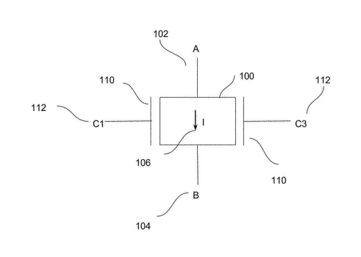
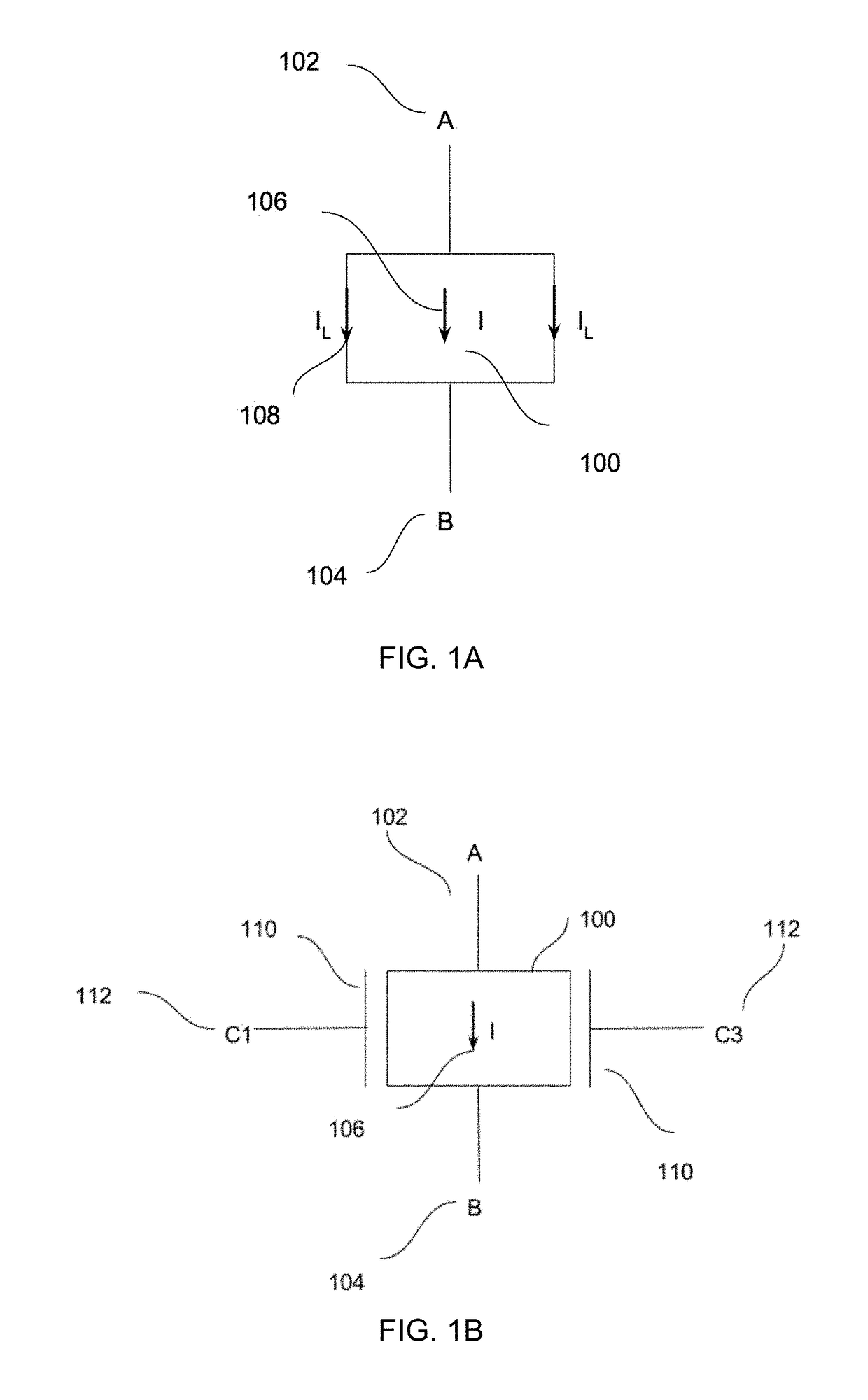
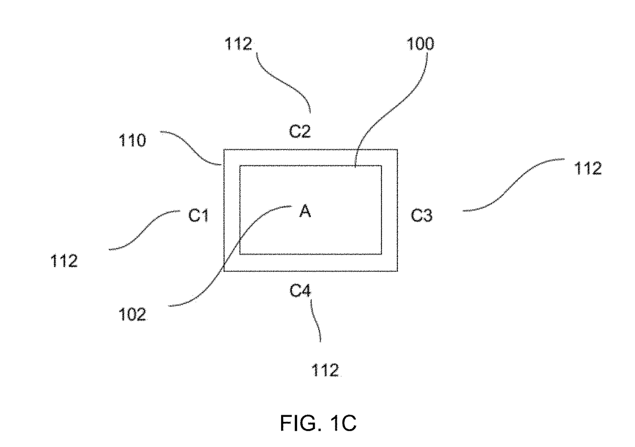
[0033]In another aspect there is provided a method of redirecting current in a current driven device comprising side walls, the method comprising: directing current through a connection pad to the device; and using a metal-insulator-semiconductor to create a field to eliminate leakage current in the side walls.

Problems solved by technology

As the size of these devices is reduced, however, device performance can start to suffer.
Patterning LED into micro size devices to create array of LEDs for display applications come with several issues including material utilization, limited PPI, and defect creation.

Method used


Image

  • Vertical solid state devices
  • Vertical solid state devices
  • Vertical solid state devices

Examples


Embodiment Construction

[0085]Unless defined otherwise, all technical and scientific terms used herein have the same meaning as commonly understood by one of ordinary skill in the art to which this invention belongs.

[0086]As used in the specification and claims, the singular forms “a,”“an” and “the” include plural references unless the context clearly dictates otherwise.

[0087]The term “comprising” as used herein will be understood to mean that the list following is non-exhaustive and may or may not include any other additional suitable items, for example one or more further feature(s), component(s) and / or element(s) as appropriate.

[0088]The terms “device” and “micro device” and “optoelectronic device” are used herein interchangeably. It would be clear to one skill in the art that the embodiments described here are independent of the device size.

[0089]The terms “donor substrate” and “temporal substrate” are used herein interchangeably. However, it is clear to one skill in the art that the embodiments descri...


PUM


Abstract

A vertical current mode solid state device comprising a connection pad and side walls comprising a metal-insulator-semiconductor (MIS) structure, wherein leakage current effect of the vertical device is limited through the side walls by biasing the MIS structure.

Description

CROSS-REFERENCE TO RELATED APPLICATIONS[0001]This application claims priority to Canadian Patent Application No. 2,924,157, filed Mar. 18, 2016 and Canadian Patent Application No. 2,916,291, filed Dec. 24, 2015, each of which is hereby incorporated by reference herein in its entirety.FIELD OF THE INVENTION[0002]The present invention pertains to vertical solid state devices, lateral conduction manipulation of vertical solid state devices, and methods of manufacture thereof. The present invention also relates to the fabrication of an integrated array of microdevices. The array of micro devices is defined by an array of contacts on a device substrate or a system substrate.BACKGROUND[0003]Integrating micro optoelectronic devices into a system substrate can offer high performance and high functionality systems. In order to improve the cost and create higher pixel density devices, the size of the optoelectronic devices should be reduced. Examples of optoelectronic devices are sensors and ...

Claims


Application Information

Patent Timeline
Patent Type & Authority Applications(United States)
IPC IPC(8): H01L33/00H01L27/15H01L33/62
CPCH01L33/0037H01L27/153H01L33/62H01L33/007H01L33/14
Inventor CHAJI, GHOLAMREZAFATHI, EHSANOLLAHSIBONI, HOSSEIN ZAMANI
Owner VUEREAL INC
Why Eureka
Try Eureka