Charge pump circuit and integrated circuit

A charge pump and circuit technology, applied in electrical components, conversion equipment without intermediate conversion to AC, and output power conversion devices, etc., can solve problems such as non-resistance of electrostatic discharge, reduce leakage current, reduce on-chip area, The effect of improving performance

Inactive Publication Date: 2008-12-03
NXP BV
View PDF1 Cites 10 Cited by
  • Summary
  • Abstract
  • Description
  • Claims
  • Application Information

AI Technical Summary

Problems solved by technology

[0007] Therefore, the above circuit does not resist electrostatic discharge on the output leads, since current sinking through a DC-DC boost or buck converter relative to a reference potential is not always possible

Method used


Image

  • Charge pump circuit and integrated circuit
  • Charge pump circuit and integrated circuit
  • Charge pump circuit and integrated circuit

Examples


Embodiment Construction

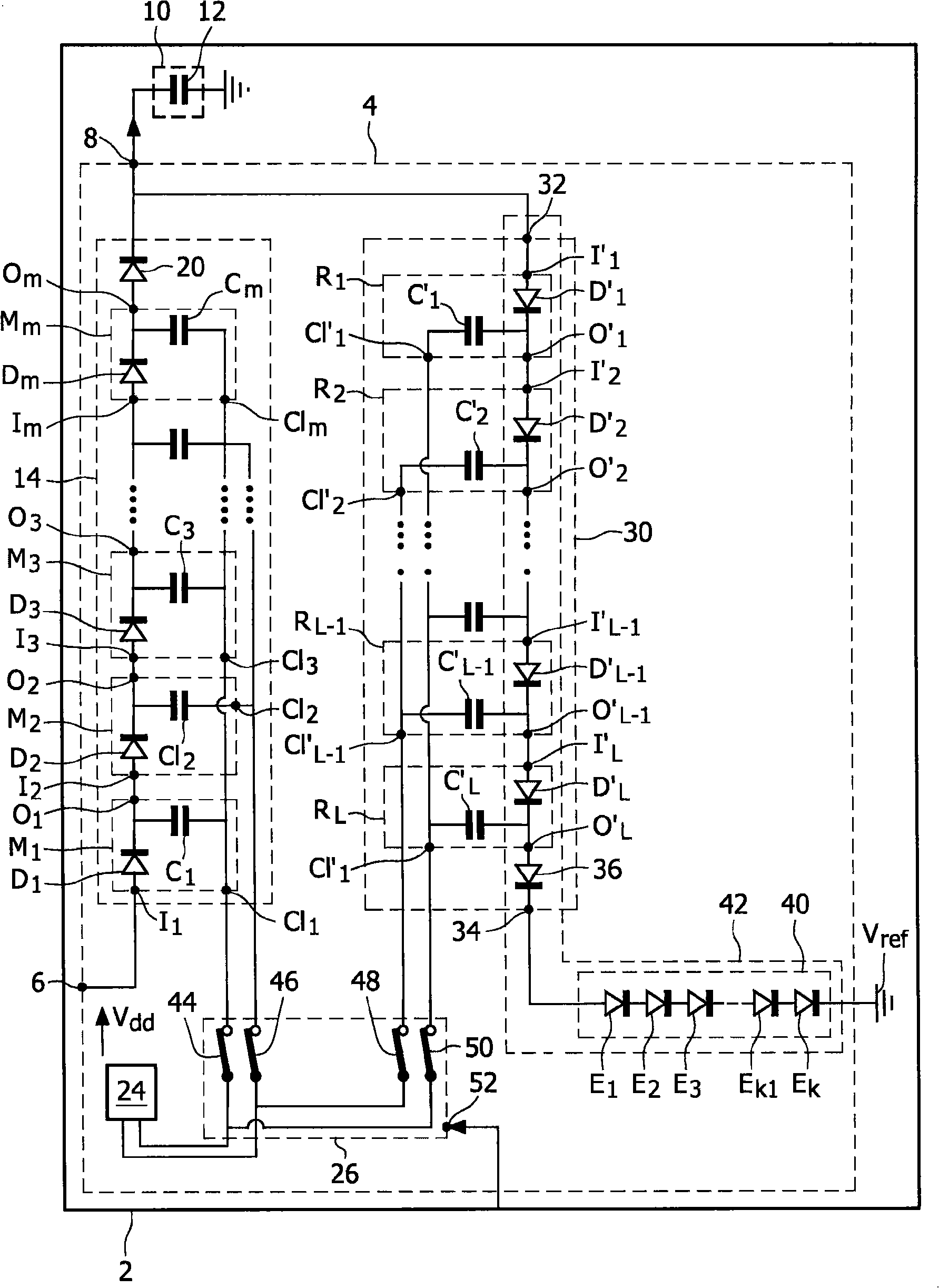
[0032] figure 1 An integrated circuit 2 is shown. Hereinafter, no detailed description will be given for functions or structures that are well known to those skilled in the art.

[0033] More precisely, figure 1 A portion of the on-chip area of ​​an integrated circuit is shown, where a charge pump circuit 4 is implemented to boost the DC circuit voltage V dd .

[0034] Circuit 4 has a function for receiving the voltage V dd The input leads 6 and for the output higher DC voltage V OUT output leads 8.

[0035] The leads 8 are connected to an on-chip load 10 . For example, load 10 is a capacitive load with capacitor 12 .

[0036] A DC-DC boost converter 14 is connected directly between leads 6 and 8 to boost lead 8 to a higher voltage V OUT .

[0037] Converter 14 is, for example, a Dickson charge pump converter. Such converters are described, for example, in the following references:

[0038] "On-chip high-voltage generation in MNOS integrated circuits using an improv...


PUM


Abstract

A charge pump circuit for increasing a circuit voltage, comprising: a DC-DC up-converter (14) having an array of capacitors arranged to charge-pump to a higher voltage than the circuit voltage, the DC-DC up-converter having an output lead (8) arranged to output the higher voltage, a DC-DC down-converter (30) connected to the output lead, the DC-DC down-converter having an array of capacitors and diodes arranged to down-pump the higher voltage, and an ESP (Electrostatic Discharge Protection) circuit comprising a series (42) of N series-connected diodes arranged to sink current from the output lead, wherein N is an integer larger than two, each diode having its anode permanently connected to the output lead and its cathode permanently connected to a reference potential, wherein the series includes the diodes of the DC-DC down-converter.

Description

technical field [0001] The invention relates to a charge pump circuit and an integrated circuit. Background technique [0002] Typically, a charge pump circuit for boosting a DC voltage circuit can include: [0003] - a DC-DC boost converter having an array of capacitors for boosting the circuit voltage to a higher voltage, a DC-DC boost converter having an output lead for outputting the higher voltage, and [0004] - A DC-DC buck converter connected to the output lead, the DC-DC buck converter having an array of capacitors and diodes for stepping down the higher voltage. [0005] The DC-DC boost converter also has a diode that prevents current from being drawn from the output lead through the DC-DC boost converter. [0006] Current sinking through the DC-DC buck converter is only possible when the DC-DC buck converter is activated. The DC-DC buck converter may only be activated when the DC-DC boost converter is disabled. [0007] Therefore, the circuit described above d...

Claims


Application Information

Patent Timeline
Patent Type & Authority Applications(China)
IPC IPC(8): H02M3/07H02M1/32
CPCH02M1/32H02M3/073
Inventor 穆罕默德·布哈玛梅让-罗伯特·图雷特卢卡·洛科科
Owner NXP BV
Why Eureka
Try Eureka