Complementary metal oxide semiconductor (CMOS) input/output interface circuit

A technology of input and output interfaces and circuits, applied in the direction of logic circuits, electrical components, pulse technology, etc., to achieve the effect of eliminating leakage current and avoiding leakage

Inactive Publication Date: 2011-05-18
SHANGHAI HUA HONG NEC ELECTRONICS
View PDF0 Cites 12 Cited by
  • Summary
  • Abstract
  • Description
  • Claims
  • Application Information

AI Technical Summary

Problems solved by technology

This loss is unsatisfactory for applications that require low power consumption circuits

Method used


Image

  • Complementary metal oxide semiconductor (CMOS) input/output interface circuit
  • Complementary metal oxide semiconductor (CMOS) input/output interface circuit
  • Complementary metal oxide semiconductor (CMOS) input/output interface circuit

Examples


Embodiment Construction

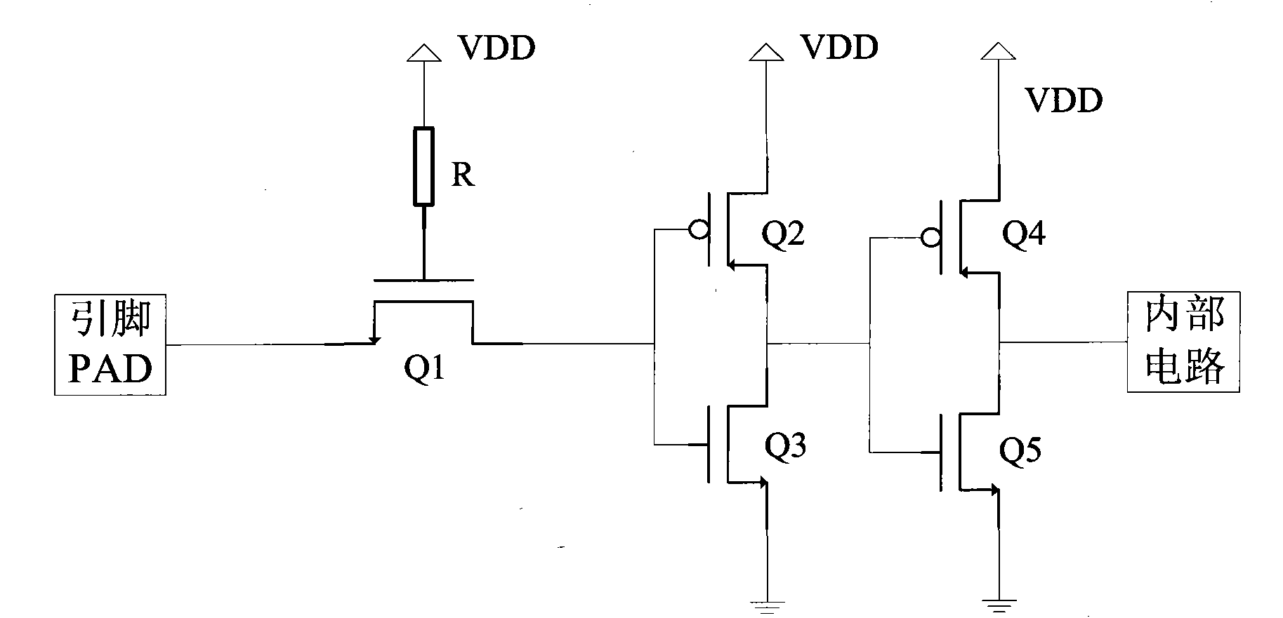
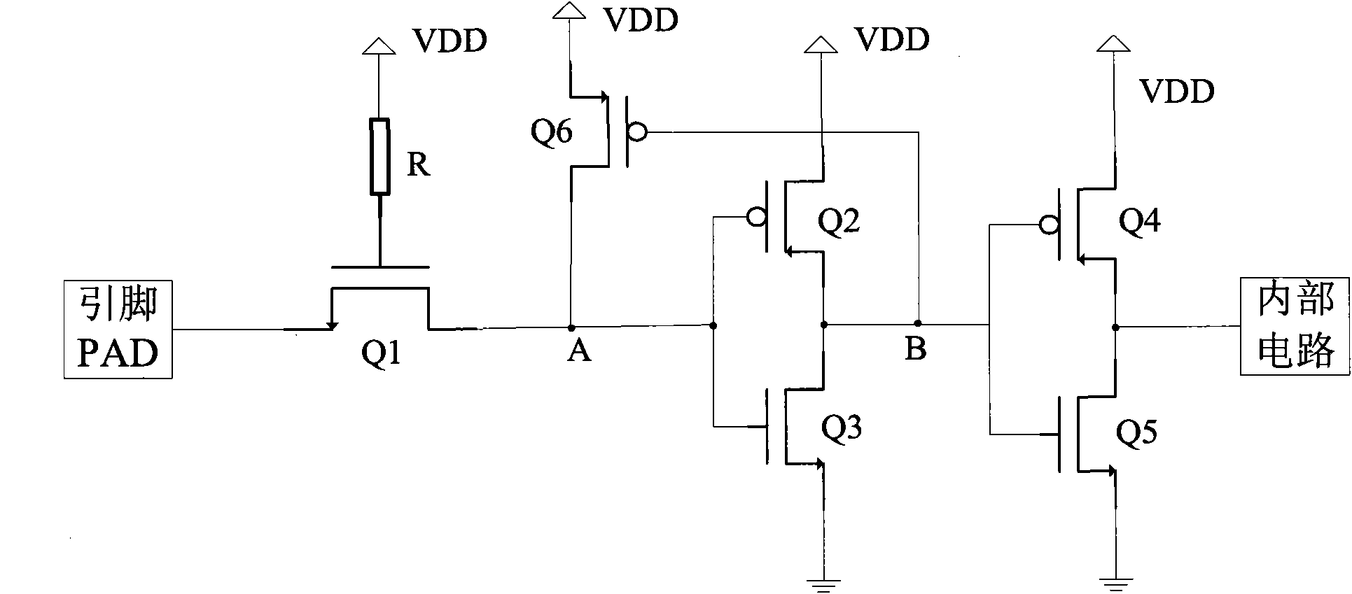
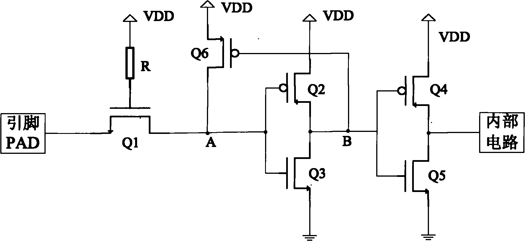
[0011] An embodiment of the CMOS input-output interface circuit of the present invention is as figure 1 As shown, it includes a first NMOS transistor Q1, a second PMOS transistor Q2, a third NMOS transistor Q3, a fourth PMOS transistor Q4, a fifth NMOS transistor Q5, a sixth PMOS transistor Q6, and a resistor R. The first NMOS transistor Q1 The gate is connected to the power supply VDD through the resistor R, the source is connected to the pin, the drain is connected to the gates of the second PMOS transistor Q2 and the third NMOS transistor Q3, the drain of the second PMOS transistor Q2 is connected to the power supply VDD, and the third NMOS transistor Q3 The source of the second PMOS transistor Q2 and the drain of the third NMOS transistor Q3 are connected to the gates of the fourth PMOS transistor Q4 and the fifth NMOS transistor Q5, and the drain of the fourth PMOS transistor Q4 is connected to the power supply VDD. The source of the fifth NMOS transistor Q5 is grounded, ...


PUM


Abstract

The invention discloses a complementary metal oxide semiconductor (CMOS) input/output interface circuit. The CMOS input/output interface circuit comprises a first N-channel metal oxide semiconductor (NMOS) transistor, a second P-channel metal oxide semiconductor (PMOS) transistor, a third NMOS transistor, a fourth PMOS transistor, a fifth NMOS transistor, a resistor and a sixth PMOS transistor, wherein the grid electrode of the first NMOS transistor is connected with a power supply through the resistor; the source electrode of the first NMOS transistor is connected with a pin; the drain electrode of the first NMOS transistor is connected with the grid electrode of the second PMOS transistor and the grid electrode of the third NMOS transistor; the drain electrode of the second PMOS transistor is connected with the power supply; the source electrode of the third NMOS transistor is grounded; the source electrode of the second PMOS transistor and the drain electrode of the third NMOS transistor are connected with the grid electrode of the fourth PMOS transistor and the grid electrode of the fifth NMOS transistor; the drain electrode of the fourth PMOS transistor is connected with the power supply; the source electrode of the fifth NMOS transistor is grounded; the source electrode of the fourth PMOS transistor and the drain electrode of the fifth NMOS transistor are connected with an internal circuit; the grid electrode of the sixth PMOS transistor is connected with the source electrode of the second PMOS transistor and the drain electrode of the third NMOS transistor; the drain electrode of the sixth PMOS transistor is connected with the grid electrode of the second PMOS transistor and the grid electrode of the third NMOS transistor; and the source electrode of the sixth PMOS transistor is connected with the power supply. The CMOS input/output interface circuit can effectively avoid the generation of leakage current.

Description

technical field [0001] The invention relates to semiconductor circuit technology, in particular to a CMOS input-output interface circuit. Background technique [0002] Typical CMOS input and output interface circuits such as figure 1 As shown, it includes a first NMOS transistor Q1, a second PMOS transistor Q2, a third NMOS transistor Q3, a fourth PMOS transistor Q2, a fifth NMOS transistor Q5, and a resistor R. The gate of the first NMOS transistor Q1 is connected to the resistor R. The power supply VDD, the source is connected to the pin, the drain is connected to the gates of the second PMOS transistor Q2 and the third NMOS transistor Q3, the drain of the second PMOS transistor Q2 is connected to the power supply VDD, the source of the third NMOS transistor Q3 is grounded, and the third NMOS transistor Q3 is connected to the ground. The source of the second PMOS transistor Q2 and the drain of the third NMOS transistor Q3 are connected to the gates of the fourth PMOS tran...

Claims


Application Information

Patent Timeline
Patent Type & Authority Applications(China)
IPC IPC(8): H03K19/0948
Inventor 徐鹏
Owner SHANGHAI HUA HONG NEC ELECTRONICS
Why Eureka
Try Eureka