Multi-layer water-splitting devices

a multi-layer, water-splitting technology, applied in the direction of electrode coating, final product manufacturing, sustainable manufacturing/processing, etc., can solve the problems of high cost, high cost, and inability to integrate a transparent polymer substrate, and achieve low cost.

Active Publication Date: 2017-07-13
AQUAHYDREX INC
View PDF5 Cites 5 Cited by
  • Summary
  • Abstract
  • Description
  • Claims
  • Application Information

AI Technical Summary

Benefits of technology

[0012]According to one aspect of the present invention there is provided a method for manufacturing (i.e. fabricating) water-splitting devices or solar cells. In a particular form, the method provides a relatively high-volume, low-cost mass-production method. In one example embodiment, the method facilitates simultaneous co-assembly of one or more sub-units and two or more polymer films or sheets to form a water-splitting device.
[0021]According to yet another aspect, water-splitting devices are manufactured using a set of readily assembled, robust sub-units which are then combined in a layered arrangement during the course of a polymer lamination process. Preferably, although not necessarily, at least one recess is provided within one or more of the laminating polymers that is specifically designed to accommodate the assembled sub-units. In a particular example form, the laminating polymers serve not only as a robust packaging device, but are integral to the assembly process itself. In another particular example form, at least one of the laminating polymers is involved in or otherwise facilitates operation of the device.

Problems solved by technology

This is often problematic however, since glass is typically fragile, heavy, expensive, and generally not well-suited to high-volume, low-cost mass-production.
One problem in this respect is to integrate a transparent polymer substrate into the fabrication of flexible electrical devices.
While techniques such as those described above are technically successful, they are typically not amenable to high volume, low-cost mass-production manufacturing, especially in respect of devices which interact with light.
The cost of manufacturing such devices may, however, be a critical factor in their physical uptake by society.
Indeed, in many cases it is purely the cost and complexity of manufacturing such devices that has halted their general use and application.
Light-modulating devices are notoriously sensitive such variations, which often destroy their utility completely.
However, no practical and economic device, or method of manufacture thereof, exists to facilitate this reaction.
The potential of solar-produced hydrogen has, consequently, never been realized.

Method used


Image

  • Multi-layer water-splitting devices
  • Multi-layer water-splitting devices
  • Multi-layer water-splitting devices

Examples


example 1

General Method for Implementation

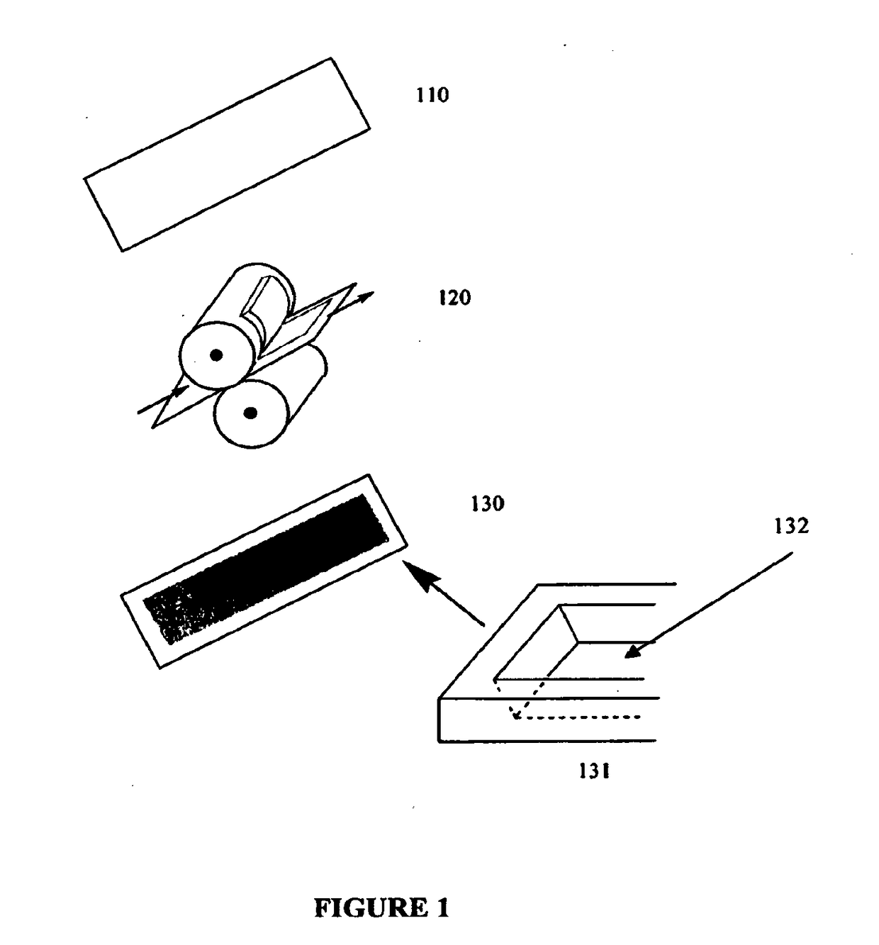
[0071]FIG. 1 illustrates a general method by which suitable recesses may be embossed or impressed into polymer films. As shown in 120, a polymer film 110 is passed between embossing rollers which contain suitable surface relief structures or protrusions, to thereby impart, under high pressure and possibly, heat, at least one recess 132, indentation, depression, cavity or the like, on the embossed or impressed polymer film 130. If desired for particular applications, a plurality of recesses can be provided in polymer film 130. It should be noted that the particular geometric shape or profile of the recess can be varied, the particular profile of recess 132 as illustrated is by way of example only.

[0072]Features can be provided within or integrated as part of the recess, for example being formed during the embossing or impressing process. Such features might include pillars, wells, further recesses, walls, protrusions and / or projections, etc.. The feat...

example 2

Fabrication of an Electrochromic Device

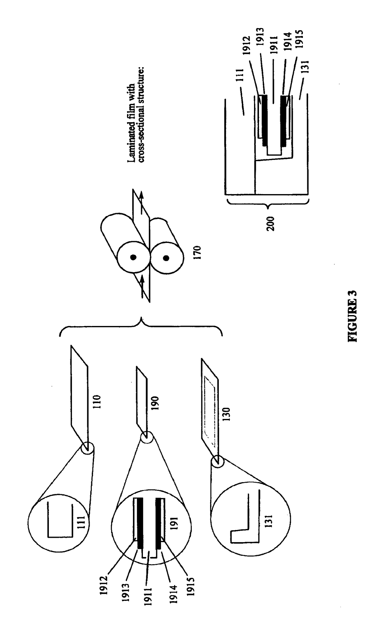
[0091]This example describes an improved method of fabrication of an electrochromic device, for example of the type described in International Publication No. WO2007002989 entitled “Charge Conducting Medium” which is incorporated herein by cross-reference.

[0092]FIG. 3 describes a method for manufacturing an electrochromic device. A PVDF membrane 1911 is coated on either side with a conducting layer, such as Ag, Pt, or ITO. The upper conducting layer 1913 is the working electrode and the lower conducting layer 1914 is the counter electrode. The upper conducting layer 1913 (working electrode) is then over-printed on the top side with a conducting polymer layer 1912, which may be PPy, PEDOT, or PANI. The lower conducting layer 1914 (counter-electrode) is overprinted with a different conducting polymer 1915, such as for example, PEDOT. The resulting sub-assembly is designated 190 in FIG. 3. Sub-assembly 190 is co-assembled with a transparent polyme...

example 3

Fabrication of a Back-Contact Dye-Sensitized Solar Cell

[0097]The top sequence in FIG. 4 depicts a method of pre-treating the working electrode in a back-contact dye-sensitized solar cell. The lower schematic in FIG. 4 depicts a process of assembling a back-contact dye-sensitized solar cell.

[0098]Referring to the top sequence in FIG. 4:

[0099]A thin, porous titanium foil 140, having cross-section 211 is dip-coated or printed with a TiO2 layer as shown in step 214. The TiO2 on the coated foil is then sintered by heating at step 215. After sintering, the foil has the cross sectional profile 211, coated with a TiO2 layer 212. The foil is then rolled up at step 216, with spacers placed between the successive layers, to thereby yield the rolled up but separated foil 217. This separated foil 217 is placed in a bath 218 containing a solution of a suitable dye such as ruthenium(II) tris(2,2′-bipyridyl) perchlorate and allowed to soak at step 219. After soaking for a period of time, for exampl...


PUM

PropertyMeasurementUnit
lengthaaaaaaaaaa
lengthaaaaaaaaaa
thicknessaaaaaaaaaa

Abstract

Water-splitting devices and methods for manufacturing water-splitting devices or solar cells is disclosed. The method seeks to provide a relatively high-volume, low-cost mass-production method. In one example, the method facilitates simultaneous co-assembly of one or more sub-units and two or more polymer films or sheets to form a water-splitting device. According to another aspect, there is provided an improved water-splitting device. In one example form, there is provided a water-splitting device which includes a first electrode for producing oxygen gas and a second electrode for producing hydrogen gas from water. The first electrode and the second electrode are positioned between a first outer polymer layer and a second outer polymer layer, and at least one spacer layer is positioned between the first outer polymer layer and the second outer polymer layer.

Description

FIELD OF THE INVENTION[0001]The present invention generally relates to water-splitting devices, such as solar cells, and in one particular aspect to improvements in the manufacture of water-splitting devices.BACKGROUND OF THE INVENTION[0002]Electrical devices that interact with light are well known. Examples include light-emitting diodes (which emit light), solar cell modules (which harvest light and turn it into electricity), and display screens (which may alter the light that they reflect). Most devices of this type use glass in one form or another as the key, transparent substrate material. This is often problematic however, since glass is typically fragile, heavy, expensive, and generally not well-suited to high-volume, low-cost mass-production. For this reason there is increasing interest in using cheaper, transparent polymeric materials in place of glass in devices of this type. Ideally, this will be combined with simple and inexpensive fabrication techniques for the devices t...

Claims


Application Information

Patent Timeline
Patent Type & Authority Applications(United States)
IPC IPC(8): H01G9/20C25B13/04C25B9/10C25B11/04C25B1/00C25B1/10C25B9/17C25B9/19C25B9/23
CPCH01G9/2004C25B1/003C25B1/10C25B9/10H01G9/2031C25B11/0447C25B13/04H01G9/2059C25B11/0415Y02E10/542C25B13/02Y02E60/36Y02P70/50C25B1/55C25B1/04C25B9/73C25B9/23C25B9/17C25B11/057C25B11/075C25B9/19
Inventor SWIEGERS, GERHARD FREDERICKOFFICER, DAVID LESLIEWALLACE, GORDON GEORGE
Owner AQUAHYDREX INC
Why Eureka
Try Eureka