Method for bonding substrates together, and substrate bonding device

a technology of substrate and bonding device, which is applied in the direction of soldering device, manufacturing tool, auxillary welding device, etc., can solve the problems of defective products and possible production of voids, and achieve the effects of preventing the production of voids between wafers, high positional precision, and suppressing strain

Active Publication Date: 2017-08-03
BONDTECH
View PDF2 Cites 35 Cited by
  • Summary
  • Abstract
  • Description
  • Claims
  • Application Information

AI Technical Summary

Benefits of technology

[0009]The present disclosure has been made in view of the foregoing circumstances, and an objective is to provide a method for bonding substrates together and a substrate bonding apparatus which are capable of preventing production of a void between substrates when the substrates are bonded together, and which are also capable of bonding those substrates together at a high positional precision.
[0013]According to an aspect of the present disclosure, in the above bonding step, the step of abutting the bonding surface of the first substrate with the bonding surface of the second substrate across the entirety of the bonding surfaces includes abutting the bonding surface of the first substrate with the bonding surface of the second substrate across the entirety of the bonding surfaces to bond the first substrate and the second substrate, decreasing the distance between the outer circumferential portion of the first substrate and the outer circumferential portion of the second substrate with distances from bottoms of the first substrate and the second substrate to the respective central portions being maintained.
[0041]According to the present disclosure, a production of a void between wafers is prevented, and a strain is suppressed, thereby enabling a bonding at a high positional precision.

Problems solved by technology

Hence, when respective flat bonding surfaces of the planar wafers are caused to face with each other and bonded, air may be trapped in between the bonding surfaces, and thus voids may be produced.
This results in a defective product.

Method used


Image

  • Method for bonding substrates together, and substrate bonding device
  • Method for bonding substrates together, and substrate bonding device
  • Method for bonding substrates together, and substrate bonding device

Examples


Embodiment Construction

[0057]An explanation will be given below of, with reference to the accompanying figures, a method for bonding substrates together, and a substrate bonding apparatus according to an embodiment based on those figures.

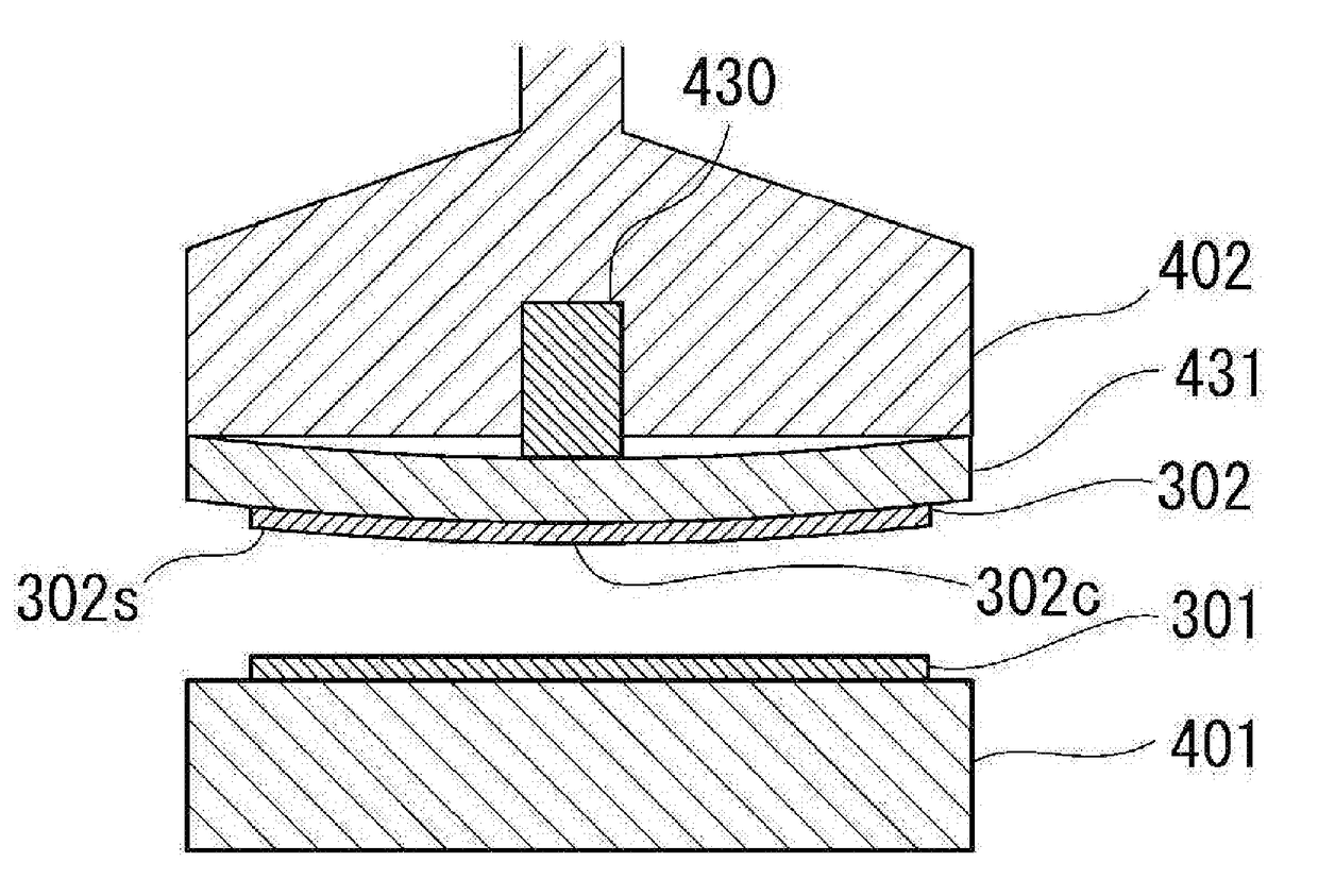
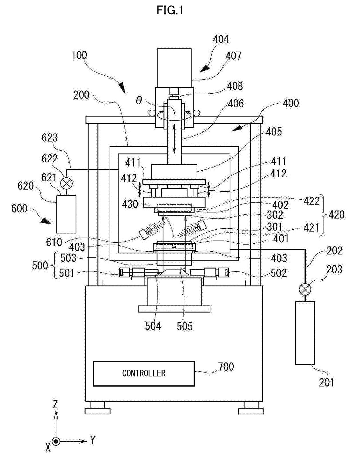
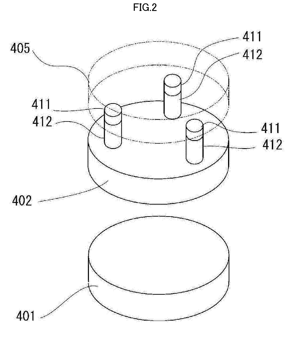
[0058]FIG. 1 is a front view illustrating a general internal structure of a substrate bonding apparatus 100 according to an embodiment of the present disclosure. FIG. 2 is a schematic perspective view illustrating a stage and the proximity of a head. FIG. 3 is a front cross-sectional view illustrating a structure of the stage that is holding a substrate. FIG. 4 is a front cross-sectional view illustrating a condition in which a substrate is bowed by a protruding mechanism provided in the stage. FIG. 5 is a front cross-sectional view of another example protruding mechanism. In order to clarify the following explanation, directions, and the like, are indicated with reference to an XYZ orthogonal coordinate system as appropriate.

[0059]As illustrated in FIG. 1, the substrate ...


PUM

PropertyMeasurementUnit
temperatureaaaaaaaaaa
timeaaaaaaaaaa

Abstract

A production of voids between substrates is prevented when the substrates are bonded together, and the substrates are bonded together at a high positional precision while suppressing a strain. A method for bonding a first substrate and a second substrate includes a step of performing hydrophilization treatment to cause water or an OH containing substance to adhere to bonding surface of the first substrate and the bonding surface of the second substrate, a step of disposing the first substrate and the second substrate with the respective bonding surfaces facing each other, and bowing the first substrate in such a way that a central portion of the bonding surface protrudes toward the second substrate side relative to an outer circumferential portion of the bonding surface, a step of abutting the bonding surface of the first substrate with the bonding surface of the second substrate at the respective central portions, and a step of abutting the bonding surface of the first substrate with the bonding surface of the second substrate across the entirety of the bonding surfaces, decreasing a distance between the outer circumferential portion of the first substrate and an outer circumferential portion of the second substrate with the respective central portions abutting each other at a pressure that maintains a non-bonded condition.

Description

TECHNICAL FIELD[0001]The present disclosure relates to a method for bonding substrates together, and a substrate bonding apparatus.BACKGROUND ART[0002]In the field of electronics, mounting technologies for bonding an electronic part with a substrate, and for bonding substrates together on which electronic circuits and electronic wirings are respectively provided are now advancing. Objects to be bonded by such mounting technologies include, on bonding surfaces, electrodes which are electrically connected to electronic circuits or the like. When the electrodes are connected together, electrical connection between the objects to be bonded is established.[0003]There are always demands for downsizing and weight reduction with respect to electronic apparatuses. In accordance with such demands, high densification and refinement of circuit patterns for an electronic circuit, and the like, are advancing. Hence, a demand for improving the alignment precision between the objects to be bonded t...

Claims


Application Information

Patent Timeline
Patent Type & Authority Applications(United States)
IPC IPC(8): H01L23/00H01L21/683H01L21/67
CPCH01L24/83H01L24/75H01L21/67259H01L21/6831H01L21/6838H01L2224/83896H01L2224/759H01L2224/8309H01L2224/75981H01L2224/83009H01L2224/757H01L2224/75102H01L2224/83908B23K20/24H01L21/68H01L2224/80012H01L2224/80013H01L2224/8013H01L2224/80132H01L2224/75702H01L2224/75705H01L2224/75701H01L2224/75305H01L2224/75303H01L2224/80047H01L2224/75272H01L2224/80893H01L2224/75724B23K37/0408B23K37/047B23K20/023B23K20/233H01L21/187H01L21/67092H01L23/544H01L21/68735H01L24/80H01L24/94H01L2223/54426H01L2224/08145H01L2224/08146H01L2224/75251H01L2224/75252H01L2224/75744H01L2224/75745H01L2224/75753H01L2224/75901H01L2224/7592H01L2224/80895H01L2224/80896H01L2224/80986H01L2224/94H01L2224/75704H01L2224/7501H01L2224/80203H01L2224/8009H01L2224/75725H01L2224/8003H01L2224/80213H01L2224/80907H01L2224/80908B23K2101/40B23K2103/50H01L2224/80009H01L2924/00012H01L2224/80H01L2924/00014H01L2224/8001H01L2224/80121B23K20/16
Inventor YAMAUCHI, AKIRA
Owner BONDTECH
Why Eureka
Try Eureka