Contact image sensor

a contact image and sensor technology, applied in the field of contact image sensors, can solve the problems of optical distortion that requires significant calibration overhead, and is unlikely to be used in portable applications, and achieve the effect of reducing the cost of the contact image sensor

Inactive Publication Date: 2017-08-03
SUNASIC TECH
View PDF6 Cites 18 Cited by
  • Summary
  • Abstract
  • Description
  • Claims
  • Application Information

AI Technical Summary

Benefits of technology

[0023]The present invention uses OLED as the light source. It makes the whole contact image sensor compact. Other than the build-in self-calibration for the uniformity of light intensity, the contact image sensor does not need optical calibration. Most important of all, the cost of the contact image sensor can be lower than that of the conventional one.

Problems solved by technology

Due to the physical space required by the components and optical path, the size of the device is usually large that it is unlikely to be used in portable applications, such as smartphones or IC cards.
Another disadvantage of the lens / prism-based optical sensor is the optical distortion that requires significant overhead to calibrate.

Method used


Image

  • Contact image sensor
  • Contact image sensor
  • Contact image sensor

Examples


Embodiment Construction

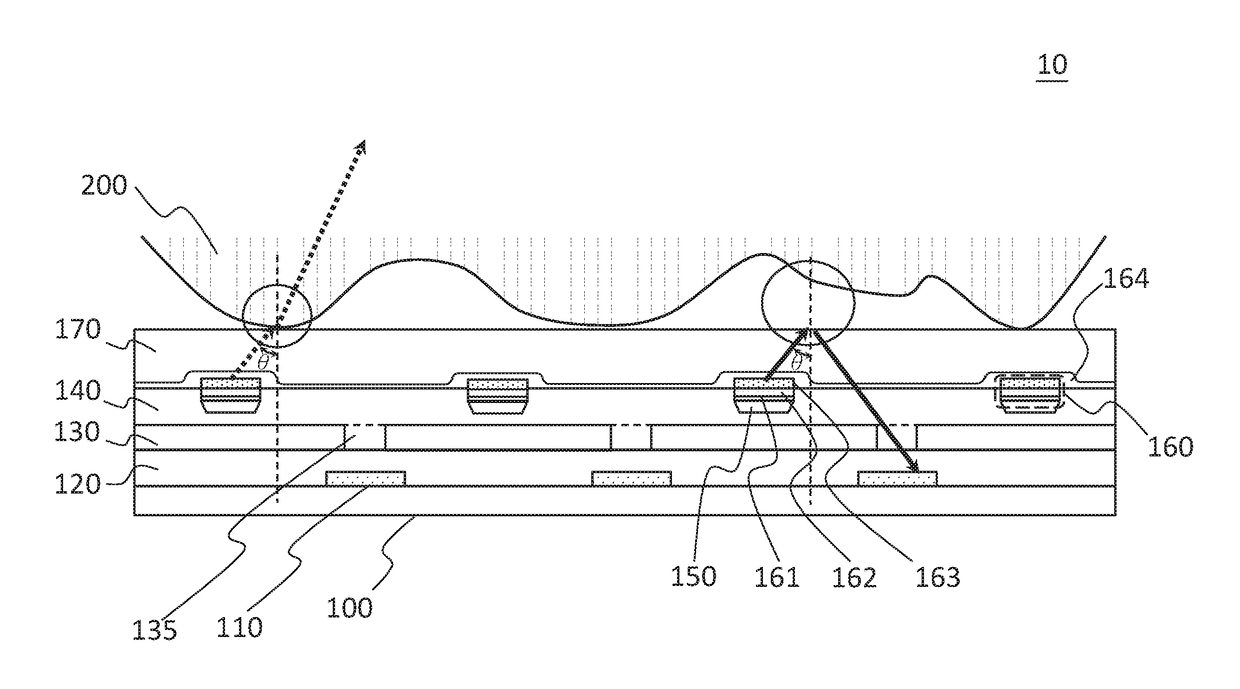
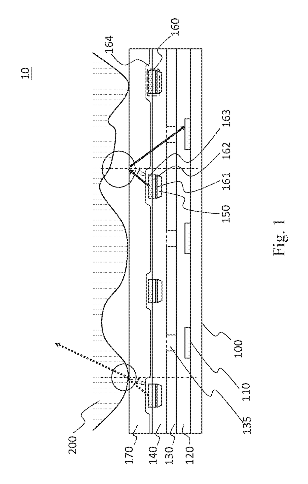
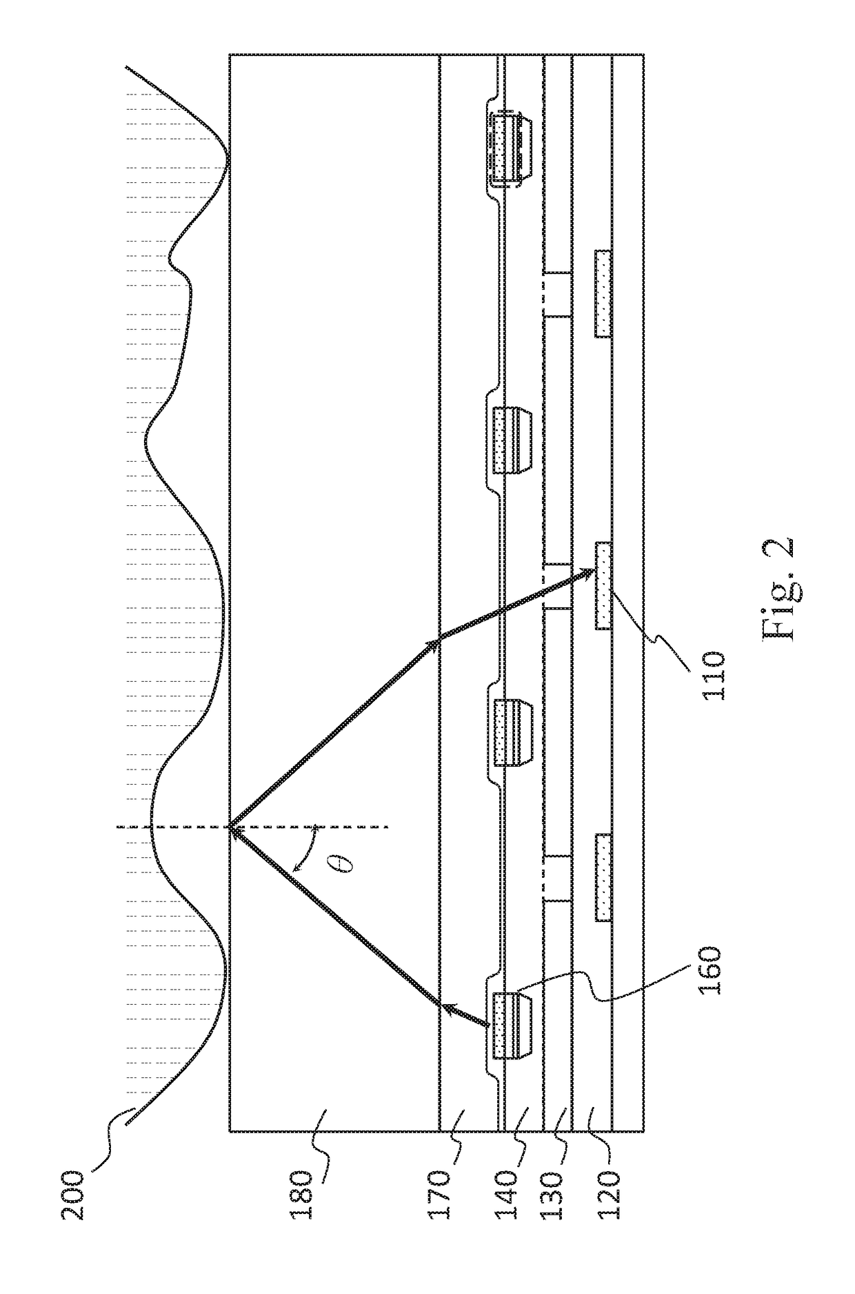
[0031]An embodiment according to the present invention is shown in FIG. 1 and FIG. 4. FIG. 1 is a perspective view of a contact image sensor 10 and FIG. 4 is a top view of the contact image sensor 10. Preferably, the contact image sensor 10 is a contact optical fingerprint sensor which can fetch users' fingerprint. The contact image sensor 10 basically includes main elements of a substrate 100, an array of sensing units 110, a first insulation structure 120, a number of focusing units 135, a second insulation structure 140, a conductive metal layer 150, an array of Organic Light-Emitting Diode (OLED) units 160 and a transparent insulation structure 170. The contact image sensor 10 may have other functional elements, such as I / O pads or logic circuits. However, these functional elements are not the key roles in the present invention and will not be described. The functionality of the main elements and the architecture of the contact image sensor 10 are illustrated below.

[0032]The sub...


PUM


Abstract

A contact image sensor is disclosed in the present invention. The contact image sensor includes: a substrate; an array of sensing units, formed above the substrate; a first insulation structure, formed over the sensing units and the substrate; a number of focusing units, formed above the first insulation structure, each focusing unit is aligned above a corresponding sensing unit with the first insulation structure sandwiched therebetween; a conductive metal layer, linked to a control circuit; an array of Organic Light-Emitting Diode (OLED) units, formed above the conductive metal layer and connected thereto; a transparent conductive layer, formed above the array of OLED units, and connected to the control circuit to control the statuses of the OLED units; and a transparent insulation structure, formed above the transparent conductive layer.

Description

FIELD OF THE INVENTION[0001]The present invention relates to a contact image sensor. Especially, the present invention relates to a contact image sensor having Organic Light-Emitting Diodes (OLED) units as a light source to obtain an image of a surface of an object. Preferably, the object is a finger and the contact image sensor works a fingerprint reader.BACKGROUND OF THE INVENTION[0002]Optical image sensors, especially fingerprint image sensors, are very popular in applications of security and personnel identification. The optical sensors capture a digital image of the fingerprint using visible or infrared light. Typical optical image sensors use light-emitting diode (LED) as a light source and a charge-coupled device (CCD) camera as a receiver, and often comprises one or more lens and prisms to form an optical path. Due to the physical space required by the components and optical path, the size of the device is usually large that it is unlikely to be used in portable applications...

Claims


Application Information

Patent Timeline
Patent Type & Authority Applications(United States)
IPC IPC(8): H01L27/146H01L27/32G06K9/00H01L27/148
CPCH01L27/14678H01L27/14625H01L27/14643G06K9/00087H01L27/14629H01L27/3227G06K9/0004H01L27/14806H01L27/14601G06V40/12G06V40/1318H10K59/60H10K50/11H10K50/15H10K50/16H10K50/828
Inventor LIN, CHI CHOUHE, ZHENG PING
Owner SUNASIC TECH
Why Eureka
Try Eureka