Image reading apparatus and semiconductor device

a reading apparatus and semiconductor technology, applied in the direction of color television, television system, radio control device, etc., can solve the problems of affecting the reliability of bonding pads or signal wiring, and affecting the reading ability of images, so as to improve the ability to read images, the effect of small drop or raise of the power source voltage due to wiring resistan

Active Publication Date: 2017-08-17
SEIKO EPSON CORP
View PDF1 Cites 2 Cited by
  • Summary
  • Abstract
  • Description
  • Claims
  • Application Information

AI Technical Summary

Benefits of technology

[0035]In the semiconductor device according to this application example, since the plurality of pixel units is arranged in a line in the direction along the first side, the power source wiring in the direction along the first side is long. However, since the analog circuit is disposed at a position which is an inner side of the logic circuit (close to the center) and is nearer to the power source pad than the logic circuit, the power source wiring from the power source pad to the analog circuit is relatively short, and the dropped or raised amount of the power source voltage due to wiring resistance is small. It is difficult to cause the analog circuit to receive an influence of power source noise occurring by a switching operation in the logic circuit. Thus, according to the semiconductor device in this application example, power is stably supplied to the analog circuit of which characteristics easily fluctuate by the power source voltage, and thus it is possible to improve capability for reading an image.

Problems solved by technology

Thus, the dropped amount of a power source voltage is large in the vicinity of the center of the chip on the long side thereof, and this may cause the characteristics to be largely degraded.
Further, since the signal wiring passes under the pads, there is a problem in reliability of bonding pads or the signal wiring.
However, since the analog circuit is disposed at a position which is an inner side of the logic circuit (close to the center of the chip) and is nearer to the power source pad than the logic circuit in the image reading chip, the power source wiring from the power source pad to the analog circuit is relatively short, and the dropped or raised amount of the power source voltage due to wiring resistance is small.
It is difficult to cause the analog circuit to receive an influence of power source noise occurring by a switching operation in the logic circuit.
Thus, propagation of power source noise occurring by the switching operation of the logic circuit is difficult, and thus it is possible to improve capability for reading an image.
Thus, both of the power source wiring from the first power source pad to the analog circuit, and the power source wiring from the second power source pad to the analog circuit are relatively short, and the dropped or raised amount of the power source voltage due to wiring resistance is small.
It is difficult to cause the analog circuit to receive an influence of power source noise occurring by a switching operation in the logic circuit.
However, since the analog circuit is disposed at a position which is an inner side of the logic circuit (close to the center) and is nearer to the power source pad than the logic circuit, the power source wiring from the power source pad to the analog circuit is relatively short, and the dropped or raised amount of the power source voltage due to wiring resistance is small.
It is difficult to cause the analog circuit to receive an influence of power source noise occurring by a switching operation in the logic circuit.

Method used


Image

  • Image reading apparatus and semiconductor device
  • Image reading apparatus and semiconductor device
  • Image reading apparatus and semiconductor device

Examples


modification example

6. Modification Example

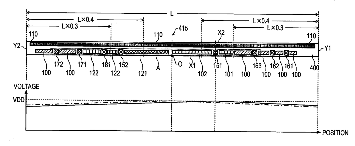
[0128]In the image reading chip 415, a positional relationship between one of the power source pads 151 and 152, and the control circuit 100, the voltage boosting circuit 101, the pixel drive circuit 102, the CDS circuit 121, and the amplification circuit 122 or the power source wirings 131, 132, 133, 134, 135, 141, 142, 143, 144, and 145 may be different from that in the exemplary embodiment. That is, the positional relationship may be established only on one side from the center of the image reading chip 415.

[0129]Hitherto, the exemplary embodiment or the modification examples are described. However, the invention is not limited to the exemplary embodiment or the modification examples, and may be implemented in various forms in the scope without departing from the gist of the invention. For example, the exemplary embodiment and the modification examples may be appropriately combined.

[0130]The invention includes substantially the same configuration (for examp...


PUM


Abstract

An image reading apparatus includes an image reading chip for reading an image. The image reading chip includes a plurality of pixel units which include a light receiving element which receives light from the image so as to perform photoelectric conversion, an analog circuit, a logic circuit, and a power source pad to which a power source voltage is supplied. The image reading chip has a shape which includes a first side and a second side shorter than the first side. A distance between the analog circuit and a median point of the first side is shorter than a distance between the logic circuit and the median point of the first side, and a distance between the analog circuit and the power source pad is shorter than a distance between the logic circuit and the power source pad.

Description

[0001]The entire disclosure of Japanese Patent Application No. 2016-025091, filed Feb. 12, 2016 is expressly incorporated by reference herein.BACKGROUND[0002]1. Technical Field[0003]The present invention relates to an image reading apparatus and a semiconductor device.[0004]2. Related Art[0005]An image reading apparatus (scanner and the like) using a contact image sensor, and a copying machine, a combination printer, or the like to which a printing function has been added have been developed. As the contact image sensor used in the image reading apparatus, a configuration of using a photodiode provided on a semiconductor substrate is used.[0006]In the contact image sensor used in the image reading apparatus such as a scanner, multiple pixel units of which each includes one or a plurality of photodiodes are disposed in line in one direction. Thus, a chip shape thereof is a very elongated rectangular shape. Because the length of a long side of the chip is determined by the size of a p...

Claims


Application Information

Patent Timeline
Patent Type & Authority Applications(United States)
IPC IPC(8): H04N1/40H04N1/401H04N5/369H04N1/031H01L27/146H01L27/148
CPCH04N1/40056H01L27/14643H01L27/14636H01L27/14825H04N2201/0081H04N5/3698H04N1/031H04N1/401H04N5/3694H04N1/484H04N25/7013H04N25/709
Inventor SUZUKI, TAKAFUMI
Owner SEIKO EPSON CORP
Why Eureka
Try Eureka