Display device

a display device and display technology, applied in static indicating devices, instruments, non-linear optics, etc., can solve the problems of difficult downsizing of display devices, affecting the operation of display devices, so as to reduce the size of the picture frame, eliminate residual electric charges, and easily supply potentials of different magnitudes

Active Publication Date: 2017-11-23
SHARP KK
View PDF2 Cites 3 Cited by
  • Summary
  • Abstract
  • Description
  • Claims
  • Application Information

AI Technical Summary

Benefits of technology

[0037]According to the first aspect of the present invention, in the display device having a layered wiring structure, for example, by supplying potentials different from each other respectively to two adjacent video signal lines using potential supply lines, it is possible to detect a leakage defect between the two video signal lines. Further, for example, by supplying a reference potential (ground potential) to all of the video signal lines using the potential supply lines when a device is turned off or terminated abnormally, it is possible to eliminate residual electric charges on the video signal lines.
[0038]According to the second aspect of the present invention, it is possible to easily supply potentials of different magnitudes to the video signal lines of the odd-numbered columns and the video signal lines of the even-numbered columns.
[0039]According to the third aspect of the present invention, since only two potential supply lines are provided, it is possible to reduce a picture-frame size. With this, it is possible to downsize the display device.
[0040]According to the fourth aspect of the present invention, by supplying potentials of different magnitudes to the video signal lines of the odd-numbered columns and the video signal lines of the even-numbered columns using the potential supply lines, the potentials of different magnitudes are supplied to any two adjacent video signal lines in the non-layered region, the potentials of different magnitudes are supplied to any two video signal lines adjacent in the vertical direction in the layered region, and the potentials of different magnitudes are supplied to any two video signal lines adjacent in the horizontal direction in the layered region. Here, in order to supply potentials of different magnitudes to the video signal lines of the odd-numbered columns and video signal lines of the even-numbered columns, two potential supply lines that serve as testing lines are sufficient. Thus, a display device having a layered wiring structure is realized, that is capable of detecting leakage without fail by using a simple circuit (testing circuit).
[0041]According to the fifth aspect of the present invention, since electric charges on the video signal lines can be eliminated when a device is turned off or terminated abnormally, for example, it is possible to suppress deterioration of display quality due to presence of a residual electric charge.
[0042]According to the sixth aspect of the present invention, in a display device having two layered regions, it is possible to achieve the same effect as that of the first aspect of the present invention.

Problems solved by technology

However, employment of a wiring structure as illustrated in FIG. 22 tends to increase a size of a picture-frame.
An increase in the size of a picture-frame as described above makes downsizing of display devices difficult.

Method used


Image

  • Display device
  • Display device
  • Display device

Examples


first embodiment

1. First Embodiment

[0073]

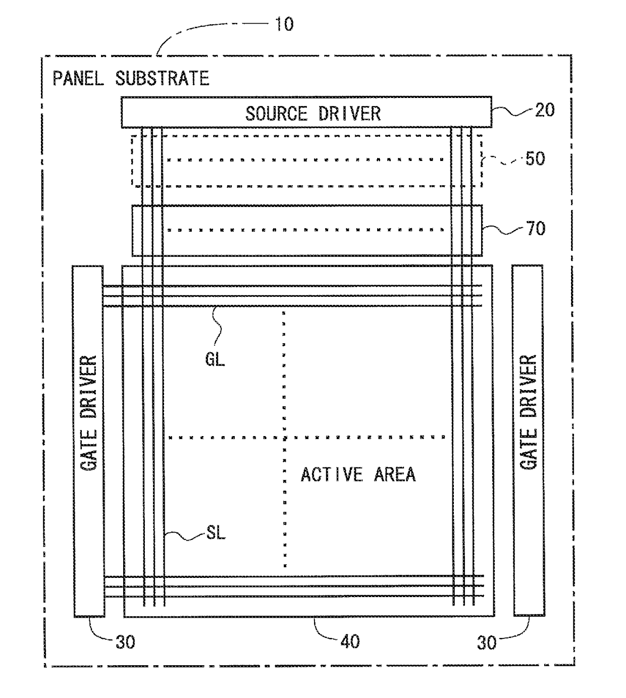
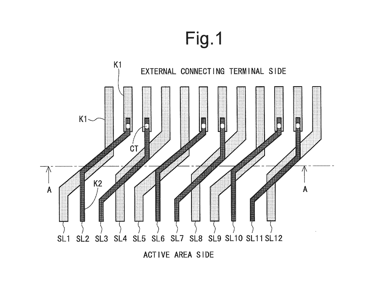
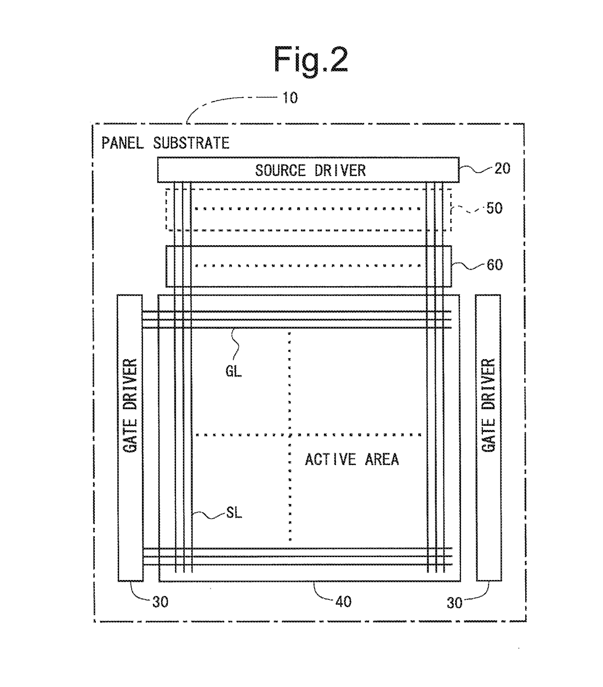
[0074]FIG. 2 is a block diagram illustrating an entire configuration of an active matrix-type liquid crystal display device according to a first embodiment of the present invention. As illustrated in FIG. 2, this liquid crystal display device is provided with a source driver 20, a gate driver 30, a testing circuit 60, and an active area (display region) 40. The active area 40, the gate driver 30, and the testing circuit 60 are provided on a panel substrate 10. Here, the panel substrate 10 in this embodiment is a glass substrate. The source driver 20 is mounted on the panel substrate 10 in a COG (Chip On Glass) manner, for example. Specifically, the source driver 20 in this embodiment is an IC chip. On the panel substrate 10, external connecting terminals for receiving video signals output from the source driver 20 which is an IC chip are provided. Here, a region indicated by a reference character 50 in FIG. 2 is a layered region (a region having a layered wi...

second embodiment

2. Second Embodiment

[0124]Next, a second embodiment of the present invention will be described.

[0125]

[0126]FIG. 19 is a block diagram illustrating an entire configuration of the active matrix-type liquid crystal display device according to a second embodiment of the present invention. The liquid crystal display device according to this embodiment is provided with a charge elimination circuit 70 in place of the testing circuit 60 in the first embodiment. The charge elimination circuit 70 is provided in a region between the active area 40 and the layered region 50. The charge elimination circuit 70 eliminates electric charges from the source bus lines SL and the pixel formation portions 4 when a device is turned off or terminated abnormally. The components other than the charge elimination circuit 70 are the same as those of the first embodiment, and therefore a description for these components will be omitted. Here, it is assumed that the wiring structure of the layered region 50 is ...


PUM

PropertyMeasurementUnit
sizeaaaaaaaaaa
insulatingaaaaaaaaaa
structureaaaaaaaaaa

Abstract

An object of the present invention is to realize a display device having a layered wiring structure, that is capable of detecting leakage without fail by using a simple testing circuit.Source bus lines (SL) are wired such that, in the layered region, two source bus lines (SL) adjacent in a vertical direction are a combination of a source bus line (SL) of an odd-numbered column and a source bus line (SL) of an even-numbered column, and two source bus lines (SL) adjacent in a horizontal direction are a combination of a source bus line (SL) of an odd-numbered column and a source bus line (SL) of an even-numbered column. Potentials of different magnitudes are supplied respectively to source bus lines (SL) of odd-numbered columns and source bus lines (SL) of even-numbered columns via testing lines.

Description

TECHNICAL FIELD[0001]The present invention relates to a display device, and more specifically to a display device having a layered wiring structure in a region between external connecting terminals on a panel substrate and an active area (display region).BACKGROUND ART[0002]A display device such as a liquid crystal display device, is provided with a large number of signal lines within a display region that is called as an active area. These signal lines are connected to external connecting terminals (terminals for receiving video signals output from a source driver IC mounted on the panel substrate, for example) disposed on a panel substrate. In the meantime, as to wiring between the active area and the external connecting terminals, as illustrated in FIG. 22, a wiring structure in a fan shape on a plane surface of the panel substrate is often employed.[0003]In recent years, demands for downsizing of display devices have become increased. However, employment of a wiring structure as...

Claims


Application Information

Patent Timeline
Patent Type & Authority Applications(United States)
IPC IPC(8): G02F1/1345G09G3/36
CPCG02F1/13458G09G2320/0214G09G3/3648
Inventor YAMAMOTO, ETSUOOHKAWA, HIROYUKIFURUTA, SHIGE
Owner SHARP KK
Why Eureka
Try Eureka