
Semiconductor devices and semiconductor systems

a technology of semiconductor devices and semiconductors, applied in the direction of coding, instruments, code conversion, etc., can solve the problem of increasing the probability of occurring errors

Active Publication Date: 2017-12-14
SK HYNIX INC
View PDF1 Cites 1 Cited by
  • Summary
  • Abstract
  • Description
  • Claims
  • Application Information

AI Technical Summary

Benefits of technology

The patent text describes a semiconductor system that includes two semiconductor devices: a first semiconductor device and a second semiconductor device. The first semiconductor device is responsible for error correction during data transmission and generates a transmission parity signal for correcting errors of a transmission data signal. The second semiconductor device is responsible for error correction during data storage and generates an internal parity signal for correcting errors of the transmission data signal and the transmission parity signal. The system selectively operates either the host error correction control circuit or the error correction control circuit based on a mode signal. The technical effect of this patent text is to provide a semiconductor system that can efficiently and accurately correct errors during data transmission and storage.

Problems solved by technology

If data transmission speeds of the semiconductor devices become faster, the probability of occurring errors may increase while the semiconductor devices are in operation.

Method used


Image

  • Semiconductor devices and semiconductor systems
  • Semiconductor devices and semiconductor systems
  • Semiconductor devices and semiconductor systems

Examples


Embodiment Construction

[0020]Various embodiments of the present disclosure will be described hereinafter with reference to the accompanying drawings. However, the embodiments described herein are for illustrative purposes only and are not intended to limit the scope of the present disclosure.

[0021]Various embodiments may be directed to semiconductor devices selecting positions in which errors of data may be corrected and semiconductor systems including the semiconductor devices.

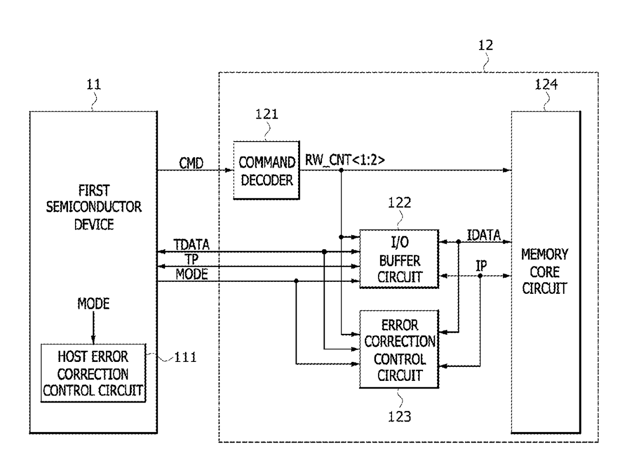
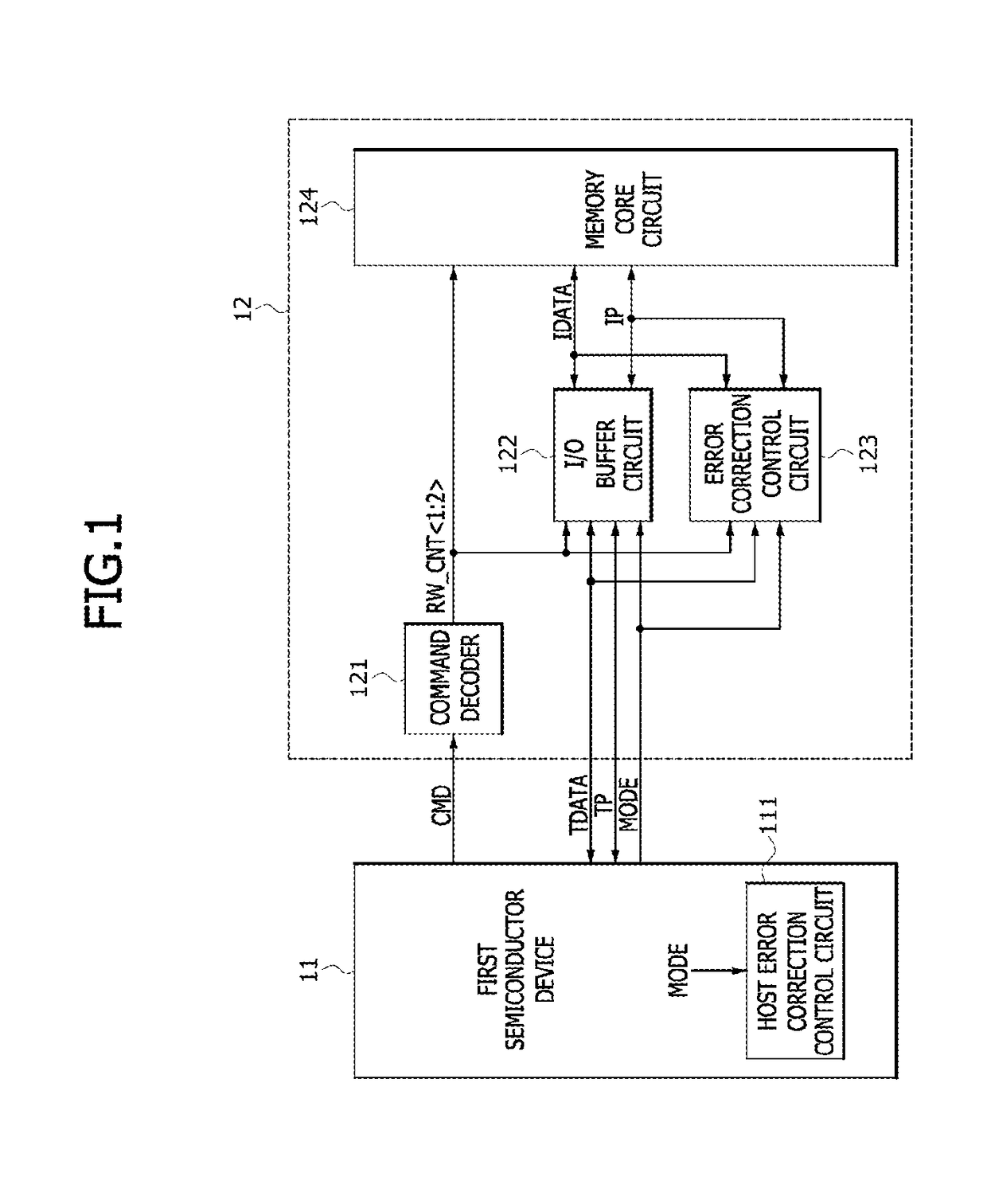
[0022]Referring to FIG. 1, a semiconductor system according to an embodiment of the present disclosure may include a first semiconductor device 11 and a second semiconductor device 12.

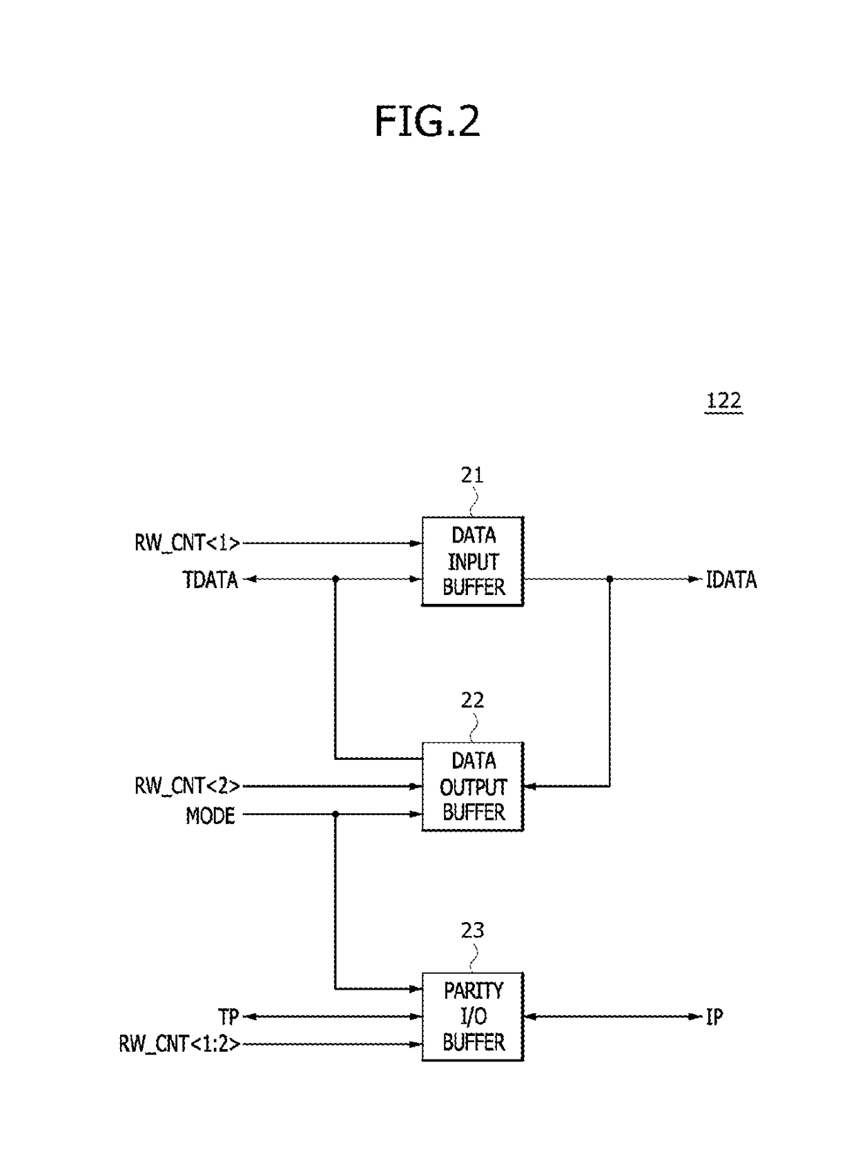
[0023]The first semiconductor device 11 may include a host error correction control circuit 111. The first semiconductor device 11 may output a command signal CMD and a mode signal MODE and may receive or output a transmission data signal TDATA and a transmission parity signal TP. The first semiconductor device 11 may output the command signal CMD, th...


PUM


Abstract

A semiconductor system may be provided. The semiconductor system may include a first semiconductor device and a second semiconductor device. The first semiconductor device may be configured to perform an error correction operation. The second semiconductor device may be configured to perform an error correction operation. The semiconductor system may selectively operate the first or second semiconductor devices with regards to error correction operations based on a mode signal.

Description

CROSS-REFERENCE TO RELATED APPLICATIONS[0001]The present application claims priority under 35 U.S.C. 119(a) to Korean Patent Application No. 10-2016-0073698, filed on Jun. 14, 2016, which is incorporated herein by reference in its entirety.BACKGROUND1. Technical Field[0002]Embodiments of the present disclosure may generally relate to semiconductor devices and semiconductor systems, and more particularly, to a semiconductor device related to the correction of errors in data.2. Related Art[0003]Recently, a DDR2 scheme or a DDR3 scheme receiving and outputting four bit data or eight bit data during each clock cycle time has been used to improve an operation speed of semiconductor devices. If data transmission speeds of the semiconductor devices become faster, the probability of occurring errors may increase while the semiconductor devices are in operation. Accordingly, novel design schemes have been proposed to improve the reliability of the data transmissions.[0004]Whenever data is tr...

Claims


Application Information

Patent Timeline
Patent Type & Authority Applications(United States)
IPC IPC(8): H03M13/11H03M13/00G11C7/22
CPCH03M13/11H03M13/6566G11C7/22G11C7/1006H03M13/13H03M13/19G06F11/1048G06F11/1032G11C29/42G11C29/022
Inventor YUN, JAE WOONGKIM, YONG MIKIM, CHANG HYUN
Owner SK HYNIX INC
Learn More