Optoelectronic semiconductor device

a technology of optoelectronic and semiconductor devices, which is applied in the field of optoelectronic semiconductor devices, can solve the problems of increasing the manufacturing accuracy of the equipment, and limiting the resolution of the optoelectronic device, so as to reduce the manufacturing time and cost and achieve higher resolution

Active Publication Date: 2017-12-21
LG DISPLAY CO LTD
View PDF8 Cites 16 Cited by
  • Summary
  • Abstract
  • Description
  • Claims
  • Application Information

AI Technical Summary

Benefits of technology

[0019]As mentioned above, in the optoelectronic semiconductor device, a plurality of microsized optoelectronic semiconductor elements are disposed apart from each other and on the epitaxial substrate, wherein the length of a side of each of the microsized optoelectronic semiconductor elements is between 1 μm and 100 μm and a minimum interval between two adjacent microsized optoelectronic semiconductor elements is 1 μm. Thereby, in comparison with the conventional optoelectronic device manufactured by LEDs, the optoelectronic semiconductor device of this invention can be applied to different fields according to the design requirement and also reduced in the manufacturing time and cost. Furthermore, the optoelectronic semiconductor devices of this invention are more suitable for the application of manufacturing the electronic device with a higher resolution, such as the VR or AR head-mounted display.

Problems solved by technology

However, with regard to the μLEDs, because they have a smaller size in the length of a side (such as 25 μm or less), when they are used to form the optoelectronic device in the manufacturing procedure the same as mentioned above, they require a higher manufacturing accuracy of the equipment and a higher cost, and therefore the manufacturing time and cost of the optoelectronic device will be increased.
Moreover, because the conventional LEDs have a larger size (the length of a side exceeds 100 μm), when they are used for manufacturing the optoelectronic device by using the above-mentioned procedure, the resolution of the optoelectronic device will be limited for being limited by the manufacturing accuracy of the equipment.

Method used


Image

  • Optoelectronic semiconductor device
  • Optoelectronic semiconductor device
  • Optoelectronic semiconductor device

Examples


Embodiment Construction

[0026]The present invention will be apparent from the following detailed description, which proceeds with reference to the accompanying drawings, wherein the same references relate to the same elements.

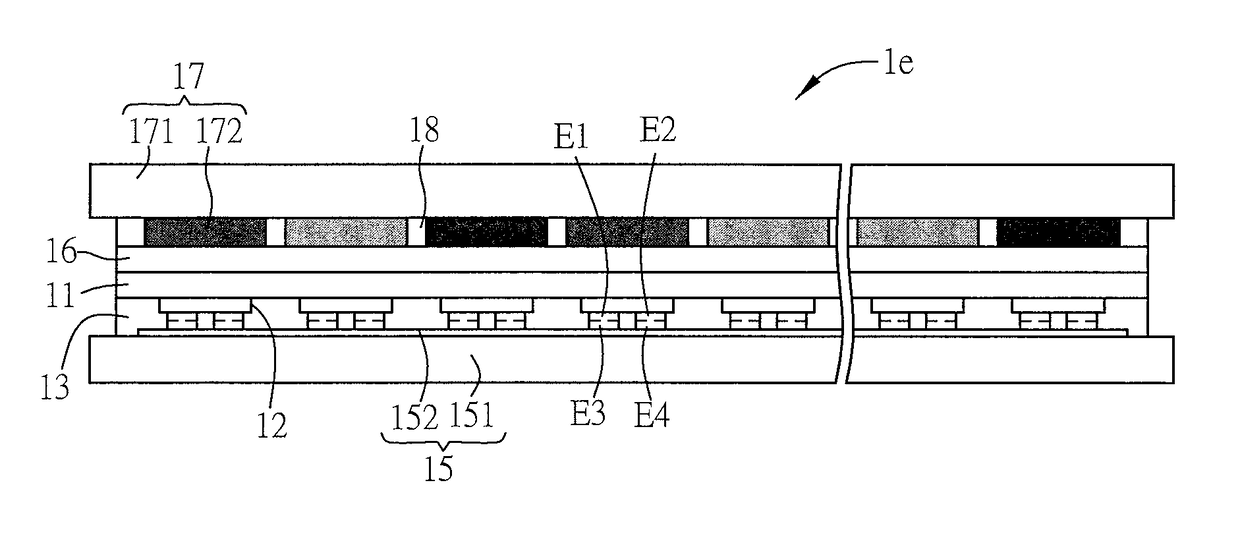
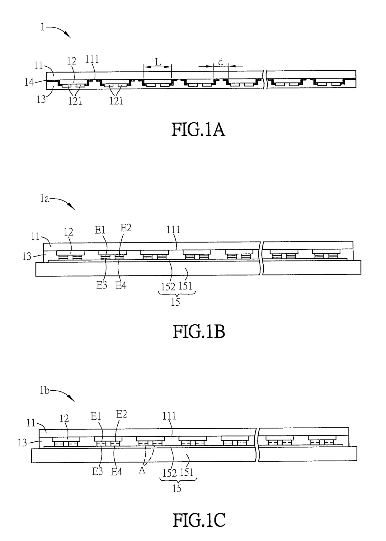
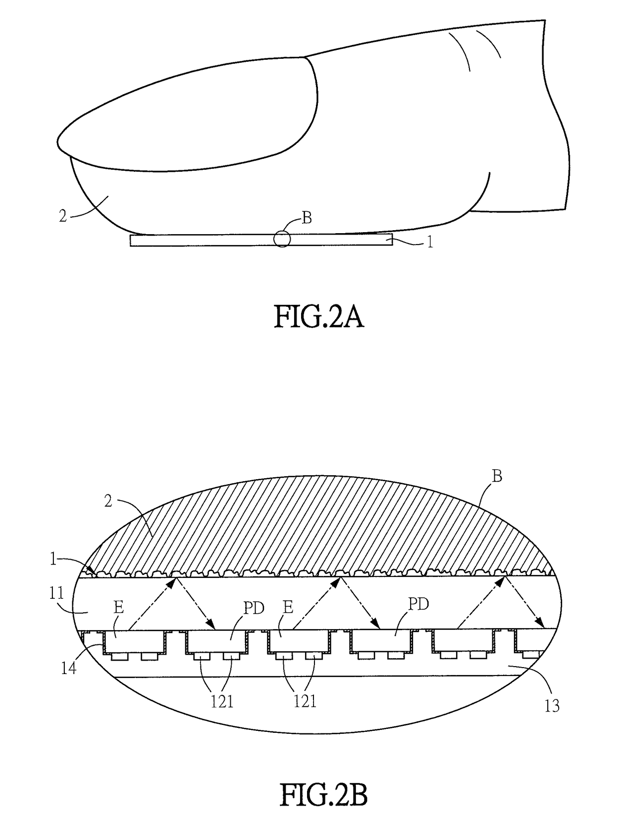
[0027]The embodiments of the optoelectronic semiconductor device of this invention will be illustrated with reference to the figures, in which the same references relate to the same elements. The all figures of the embodiments are given for illustration only and not for representing the actual size and ratio. Besides, the terms used to describe the position such as “up” and “down” are only for representing the relative position. Moreover, the description of that one element is formed “on”, “above”, “below”, or “under” another element can comprise one embodiment wherein one element directly contacts another element or another embodiment where an additional element is disposed between one element and another element so that the one element and the another element don't contact each othe...


PUM


Abstract

An optoelectronic semiconductor device includes an epitaxial substrate and a plurality of microsized optoelectronic semiconductor elements. The microsized optoelectronic semiconductor elements are disposed separately and disposed on a surface of the epitaxial substrate. A length of a side of each of the microsized optoelectronic semiconductor elements is between 1 μm and 100 μm, and a minimum interval between two adjacent microsized optoelectronic semiconductor elements is 1 μm.

Description

CROSS REFERENCE TO RELATED APPLICATIONS[0001]This Non-provisional application claims priority under 35 U.S.C. §119(a) on Patent Application No(s). 105119178 filed in Taiwan, Republic of China on Jun. 17, 2016, the entire contents of which are hereby incorporated by reference.BACKGROUND OF THE INVENTIONField of Invention[0002]The invention relates to a semiconductor device and, in particular, to an optoelectronic semiconductor device.Related Art[0003]In comparison with the conventional liquid crystal display device, the micro LED array display composed of micro LEDs (μLEDs) is more contributive to the purposes of lightness and thinness because it doesn't require an additional backlight source.[0004]In the conventional procedure of manufacturing an optoelectronic device (such as a display) by using LEDs (the length of a side is greater than 100 μm), the epitaxial process is used to form LEDs, and then the half cutting (electrical insulation), probing and full cutting are performed to ...

Claims


Application Information

Patent Timeline
Patent Type & Authority Applications(United States)
IPC IPC(8): H01L25/16H01L33/50H01L33/36H01L33/00H01L31/0232H01L31/0224H01L31/02H01L27/12H01L33/62H01L31/173G06K9/00
CPCH01L25/167H01L33/0095H01L31/02005H01L31/173H01L27/1214G06K9/0004H01L31/02322H01L31/02327H01L33/36H01L33/505H01L33/62H01L31/022408H01L27/156H01L25/0753G06V40/1318
Inventor CHEN, HSIEN-TE
Owner LG DISPLAY CO LTD
Why Eureka
Try Eureka