Method of making a semiconductor chip assembly with a bumped metal pillar

a metal pillar and semiconductor chip technology, applied in semiconductor devices, semiconductor/solid-state device details, electrical devices, etc., can solve the problems of significant cost and technical limitations, over-all cost saving, and significant cost of forming bumps on the pads, so as to reduce stress, facilitate manufacturing, and enhance mechanical support and protection

Inactive Publication Date: 2006-09-26
BRIDGE SEMICON
View PDF150 Cites 11 Cited by
  • Summary
  • Abstract
  • Description
  • Claims
  • Application Information

AI Technical Summary

Benefits of technology

[0062]An advantage of the present invention is that the semiconductor chip assembly can be manufactured conveniently and cost effectively. Another advantage is that the encapsulant can be provided before the metal base is etched to form the metal pillar, thereby enhancing mechanical support and protection for the routing line and the bumped terminal. Another advantage is that the metal pillar can cover the bumped terminal while the metal base is etched to form the metal pillar, thereby reducing stress between the routing line and the bumped terminal and improving reliability. Another advantage is that the metal pillar can be formed by etching (subtractively) rather than by electroplating or electroless plating (additively) which improves uniformity and reduces manufacturing time and cost. Another advantage is that the connection joint can be made from a wide variety of materials and processes, thereby making advantageous use of mature connection joint technologies in a unique and improved manufacturing approach. Another advantage is that the assembly need not include wire bonds or TAB leads, although the process is flexible enough to accommodate these techniques if desired. Another advantage is that the assembly can be manufactured using low temperature processes which reduces stress and improves reliability. A further advantage is that the assembly can be manufactured using well-controlled processes which can be easily implemented by circuit board, lead frame and tape manufacturers. Still another advantage is that the assembly can be manufactured using materials that are compatible with copper chip and lead-free environmental requirements.
[0063]These and other objects, features and advantages of the invention will be further described and more readily apparent from a review of the detailed description of the preferred embodiments which follows.

Problems solved by technology

In addition, flip-chip bonding requires minimal mounting area and weight which results in overall cost saving since no extra packaging and less circuit board space are used.
While flip-chip technology has tremendous advantages over wire bonding and TAB, its cost and technical limitations are significant.
For instance, the cost of forming bumps on the pads is significant.
In addition, an adhesive is normally underfilled between the chip and the support circuit to reduce stress on the solder joints due to thermal mismatch between the chip and the support circuit, and the underfilling process increases both manufacturing complexity and cost.
The plating bus creates design constraints and must be removed after the electroplating occurs.
Non-uniform plating may arise at the bottom of relatively deep through-holes due to poor current density distribution.
Furthermore, the electrolytic bath is relatively expensive.
However, electroless plating is relatively slow.
Furthermore, the electroless bath is relatively expensive.
Further, the solder is typically a tin-lead alloy and lead-based materials are becoming far less popular due to environmental concerns over disposing of toxic materials and leaching of toxic materials into ground water supplies.
Moisture penetration through the polymer binder may induce corrosion or oxidation of the conductive filler particles resulting in an unstable electrical connection.
Furthermore, the polymer binder and the conductive filler may degrade leading to an unstable electrical connection.
Thus, the conductive adhesive may have adequate mechanical strength but poor electrical characteristics.
Thermo-mechanical wear or creep of the solder joints that connect the semiconductor chip assembly to the next level assembly is a major cause of failure in most board assemblies.
This is because non-uniform thermal expansion and / or contraction of different materials causes mechanical stress on the solder joints.
However, due to large transient temperature differences between the chip and other materials during power-up of the system, the induced solder joint stress makes the assembly unreliable even when the chip and the other materials have closely matched thermal expansion coefficients.
A drawback to this approach is that when the wire bonder forms the gold ball on the pad it applies substantial pressure to the pad which might destroy active circuitry beneath the pad.
In addition, gold from the pin can dissolve into the solder to form a gold-tin intermetallic compound which mechanically weakens the pin and therefore reduces reliability.
Since photoresist is not fully transparent and tends to absorb the light, the thicker the photoresist, the poorer the penetration efficiency of the light.
As a result, the lower portion of the photoresist might not receive adequate light to initiate or complete the intended photo-reaction.
Consequently, the bottom portion of the opening in the photoresist might be too narrow, causing a pillar formed in the narrowed opening to have a diameter that decreases with decreasing height.
Such a pillar has a high risk of fracturing at its lower portion in response to thermally induced stress.
Furthermore, photoresist residue on the underlying metal might cause the pillar to have poor quality or even prevent the pillar from being formed.
Second, if the photoresist is relatively thick (such as 100 microns or more), the photoresist may need to be applied with multiple coatings and receive multiple light exposures and bakes, which increases cost and reduces yield.
Third, if the photoresist is relatively thick, the electroplated pillar may be non-uniform due to poor current density distribution in the relatively deep opening.

Method used


Image

  • Method of making a semiconductor chip assembly with a bumped metal pillar
  • Method of making a semiconductor chip assembly with a bumped metal pillar
  • Method of making a semiconductor chip assembly with a bumped metal pillar

Examples


Embodiment Construction

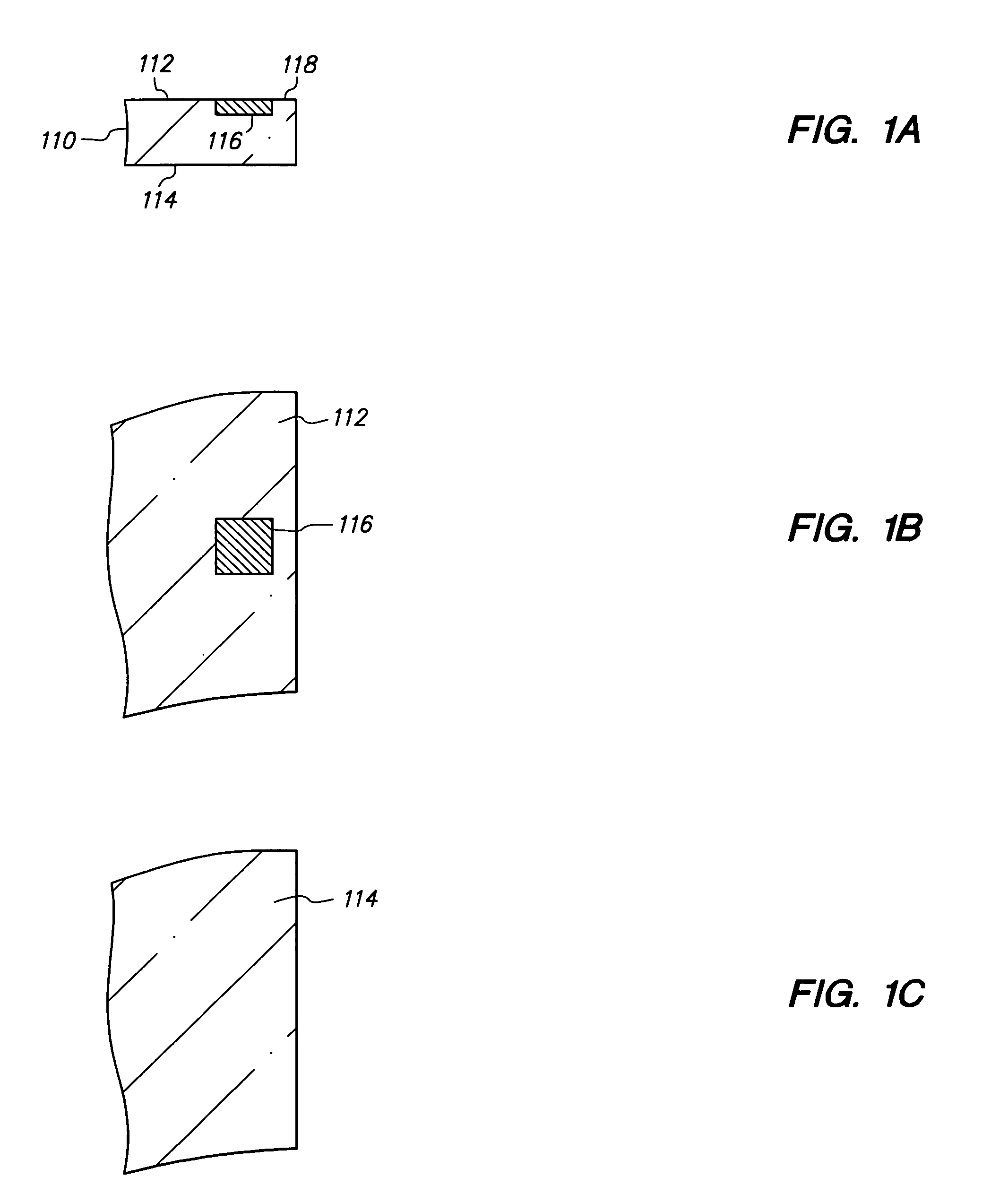
[0077]FIGS. 1A–21A, 1B–21B and 1C–21C are cross-sectional, top and bottom views, respectively, of a method of making a semiconductor chip assembly in accordance with a first embodiment of the present invention.

[0078]FIGS. 1A, 1B and 1C are cross-sectional, top and bottom views, respectively, of semiconductor chip 110 which is an integrated circuit in which various transistors, circuits, interconnect lines and the like are formed (not shown). Chip 110 includes opposing major surfaces 112 and 114 and has a thickness (between surfaces 112 and 114) of 150 microns. Surface 112 is the active surface and includes conductive pad 116 and passivation layer 118.

[0079]Pad 116 is substantially aligned with passivation layer 118 so that surface 112 is essentially flat. Alternatively, if desired, pad 116 can extend above or be recessed below passivation layer 118. Pad 116 provides a bonding site to electrically couple chip 110 with external circuitry. Thus, pad 116 can be an input / output pad or a ...


PUM


Abstract

A method of making a semiconductor chip assembly includes providing a metal base, a routing line and a bumped terminal, then mechanically attaching a semiconductor chip to the metal base, the routing line and the bumped terminal, then forming an encapsulant, and then etching the metal base to form a metal pillar that contacts the bumped terminal.

Description

CROSS-REFERENCE TO RELATED APPLICATIONS[0001]This application is a continuation of U.S. application Ser. No. 10 / 994,604 filed Nov. 22, 2004, which is a continuation-in-part of U.S. application Ser. No. 10 / 922,280 filed Aug. 19, 2004, which is a continuation-in-part of U.S. application Ser. No. 10 / 307,218 filed Nov. 29, 2002, and issued as U.S. Pat. No. 6,809,414 which is a divisional of U.S. application Ser. No. 09 / 997,973 filed Nov. 29, 2001, and issued as U.S. Pat. No. 6,492,252 which is a continuation-in-part of U.S. application Ser. No. 09 / 917,339 filed Jul. 27, 2001, U.S. Pat. No. 6,537,851 which is a continuation-in-part of U.S. application Ser. No. 09 / 878,626 filed Jun. 11, 2001, and issued as U.S. Pat. No. 6,653,217 which is a continuation-in-part of U.S. application Ser. No. 09 / 687,619 filed Oct. 13, 2000, and issued as U.S. Pat. No. 6,440,835 each of which is incorporated by reference.[0002]U.S. application Ser. No. 10 / 994,604 filed Nov. 22, 2004 also claims the benefit of...

Claims


Application Information

Patent Timeline
Patent Type & Authority Patents(United States)
IPC IPC(8): H01L21/44
CPCH01L21/4832H01L21/4846H01L21/6835H01L23/3107H01L23/49827H01L24/32H01L24/48H01L24/83H01L24/29H01L24/45H01L24/81H01L24/85H01L2221/68377H01L2224/16H01L2224/32057H01L2224/45144H01L2224/48091H01L2224/48227H01L2224/48465H01L2224/48599H01L2224/73265H01L2224/8121H01L2224/81815H01L2224/83121H01L2224/83192H01L2224/83194H01L2224/83385H01L2224/83856H01L2924/01005H01L2924/01011H01L2924/01012H01L2924/01013H01L2924/01014H01L2924/01015H01L2924/01022H01L2924/01028H01L2924/01029H01L2924/0103H01L2924/0104H01L2924/01046H01L2924/01047H01L2924/0105H01L2924/01074H01L2924/01078H01L2924/01079H01L2924/01082H01L2924/01202H01L2924/01203H01L2924/01327H01L2924/014H01L2924/07802H01L2924/09701H01L2924/14H01L2924/19041H01L2924/19043H01L2924/3025H01L2224/2919H01L2224/32145H01L2924/01006H01L2924/01019H01L2924/01024H01L2924/01033H01L2924/0665H01L2924/0132H01L2924/0134H01L2224/85H01L2924/1579H01L2224/45124H01L2224/29111H01L2224/32225H01L2924/15311H01L2224/73204H01L2924/3651H01L2924/00014H01L2924/00H01L2924/01026H01L2924/3512H01L2924/00015H01L2224/13111H01L2924/00012H01L2924/351H01L2224/45147H01L2224/05554H01L2224/29101H01L2924/181H01L2224/45155H01L2224/45164H01L2224/85207H01L2224/45111H01L2224/0401H01L24/73H01L2224/05655H01L2224/05624
Inventor LIN, CHARLES W. C.CHIANG, CHENG-LIEN
Owner BRIDGE SEMICON
Why Eureka
Try Eureka