
Display device

a display device and display technology, applied in the field of display devices, can solve the problems of increasing parasitic capacitance of driving tft, and achieve the effects of reducing off-current, preventing the occurrence of parasitic capacitance, and high quality

Active Publication Date: 2017-12-21
SAMSUNG DISPLAY CO LTD
View PDF4 Cites 15 Cited by
  • Summary
  • Abstract
  • Description
  • Claims
  • Application Information

AI Technical Summary

Benefits of technology

The patent aims to reduce the gap between elements of a TFT and wiring in a display device to achieve higher resolution or miniaturization. However, this often results in an increase in parasitic capacitance, which negatively affects the image quality. The invention proposes a solution to prevent this issue and provide a better image quality by reducing the off-current. The technical effect is to enhance the image quality of display devices by reducing parasitic capacitance.

Problems solved by technology

According to a display device of the related art, as intervals between elements of a thin film transistor (“TFT”) and / or wirings of a display device are reduced so as to implement a miniaturized or high resolution display device, disadvantages such as parasitic capacitance of a driving TFT have increased.

Method used


Image

  • Display device
  • Display device
  • Display device

Examples


Embodiment Construction

[0031]As the disclosure allows for various changes and numerous exemplary embodiments, exemplary embodiments will be illustrated in the drawings and described in detail in the written description. An effect and a characteristic of the disclosure, and a method of accomplishing these will be apparent when referring to exemplary embodiments described with reference to the drawings. This disclosure may, however, be embodied in many different forms and should not be construed as limited to the exemplary embodiments set forth herein.

[0032]Hereinafter, the disclosure will be described more fully with reference to the accompanying drawings, in which exemplary embodiments of the disclosure are shown. When description is made with reference to the drawings, like reference numerals in the drawings denote like or corresponding elements, and repeated description thereof will be omitted.

[0033]As used herein, the term “and / or” includes any and all combinations of one or more of the associated list...


PUM


Abstract

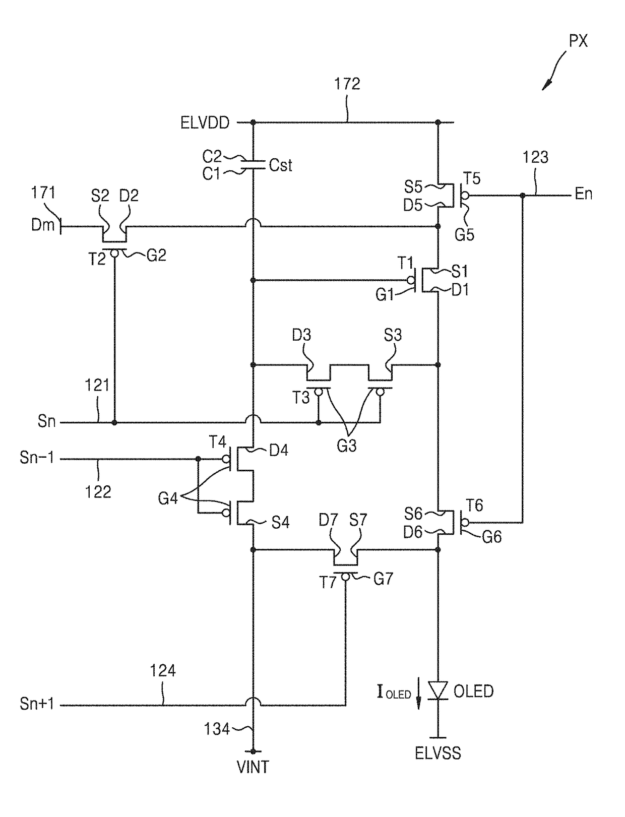
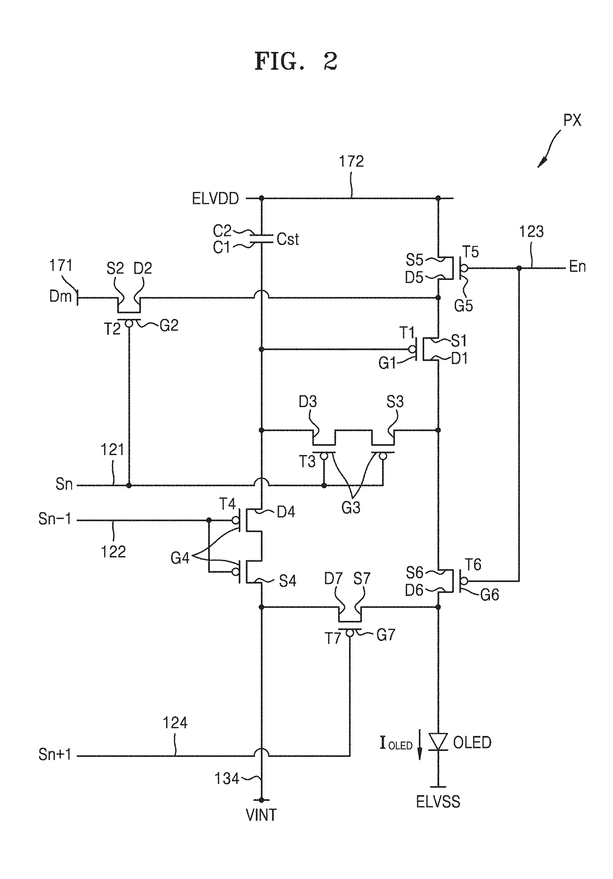
A display device includes a scan line extending in a first direction, a data line and a driving voltage line extending in a second direction crossing the first direction, a switching thin film transistor (“TFT”) connected to the scan line and the data line, a driving TFT connected to the switching TFT and including a driving semiconductor layer and a driving gate electrode, a storage capacitor connected to the driving TFT and including first and second storage capacitor plates, a node connection line between the data line and the driving voltage line and connected to the driving gate electrode, and a shielding portion between the data line and the node connection line.

Description

[0001]This application claims priority to Korean Patent Application No. 10-2016-0074732, filed on Jun. 15, 2016, and all the benefits accruing therefrom under 35 U.S.C. §119, the content of which in its entirety is herein incorporated by reference.BACKGROUND1. Field[0002]One or more exemplary embodiments relate to a display device.2. Description of the Related Art[0003]Generally, a display device includes a display element and electronic elements for controlling an electrical signal to be applied to the display element. The electronic elements include a thin film transistor (“TFT”), a storage capacitor, and a plurality of wirings.[0004]To accurately control an emission and an emission degree of a display element, a number of TFTs electrically connected to one display element has increased and a number of the plurality of wirings transferring an electrical signal to the TFTs has also increased.SUMMARY[0005]According to a display device of the related art, as intervals between element...

Claims


Application Information

Patent Timeline
Patent Type & Authority Applications(United States)
IPC IPC(8): H01L27/32H01L27/12G09G3/3258
CPCH01L27/3225H01L27/1255G09G3/3258G09G2300/0819G09G2300/0426G09G2300/043G09G2300/0842G09G3/3225G09G3/3233G09G2300/0861G09G2310/0251G09G2310/0262G09G2320/043H10K59/126H10K59/131H10K59/00
Inventor CHOI, JUNWONIN, YUNKYEONGHWANG, WONMIAN, JUNYONG
Owner SAMSUNG DISPLAY CO LTD
Learn More