Electronic component device, method of mounting electronic component device on circuit board, and mounting structure of electronic component device on circuit board

Active Publication Date: 2018-01-04
MURATA MFG CO LTD
View PDF3 Cites 32 Cited by
  • Summary
  • Abstract
  • Description
  • Claims
  • Application Information

AI Technical Summary

Benefits of technology

[0045]An electronic component device according to a preferred embodiment of the present invention is capable of being reliably mounted on, for example, a circuit board without connection failure by previously making large the thickness of the sealing resin layer at a region that tends to be raised after mounting the electronic component device.
[0046]A method of mounting an electronic component device on a circuit board according to a preferred embodiment of the present invention also makes it possible to reliably mount the electronic component device on the circuit board withou

Problems solved by technology

That is, joining failure sometimes occurs due to the areas (formation densities) of the outer electrodes in the regions not being equal to eac

Method used


Image

  • Electronic component device, method of mounting electronic component device on circuit board, and mounting structure of electronic component device on circuit board
  • Electronic component device, method of mounting electronic component device on circuit board, and mounting structure of electronic component device on circuit board
  • Electronic component device, method of mounting electronic component device on circuit board, and mounting structure of electronic component device on circuit board

Examples


first preferred embodiment

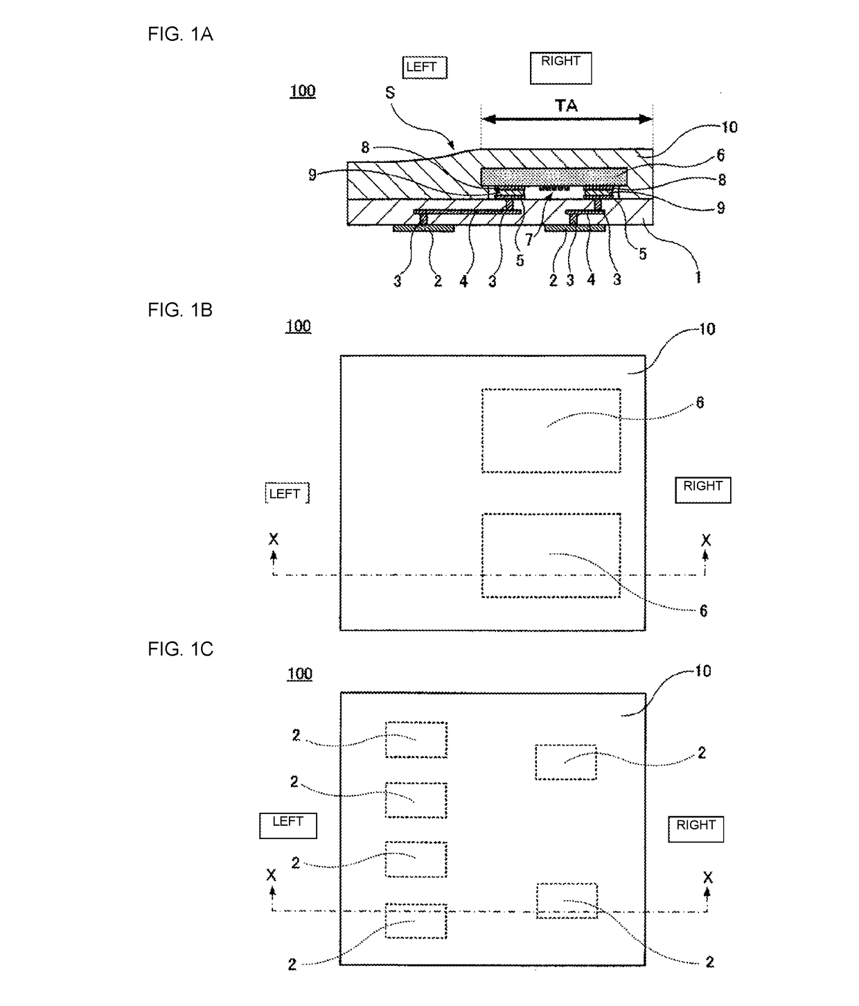
[0069]FIGS. 1A to 1C illustrate an electronic component device 100 according to a first preferred embodiment of the present invention. FIG. 1A is a sectional view of the electronic component device 100. FIG. 1B is a plan view of the electronic component device 100, and also shows in perspective built-in substrate components 6. FIG. 1C is also a plan view of the electronic component device 100, and also shows in perspective outer electrodes 2 that are on a lower principal surface. The sectional view of FIG. 1A shows a portion taken along a dash-dot line X-X in each of FIGS. 1B and 1C.

[0070]The electronic component device 100 is preferably a surface acoustic wave device, for example.

[0071]The electronic component device 100 includes a mount substrate 1. The mount substrate 1 is preferably made of ceramic, such as alumina. However, the mount substrate 1 may be made of any material, such as glass ceramic or resin, instead of ceramic.

[0072]The outer electrodes 2 are provided on the lower...

second preferred embodiment

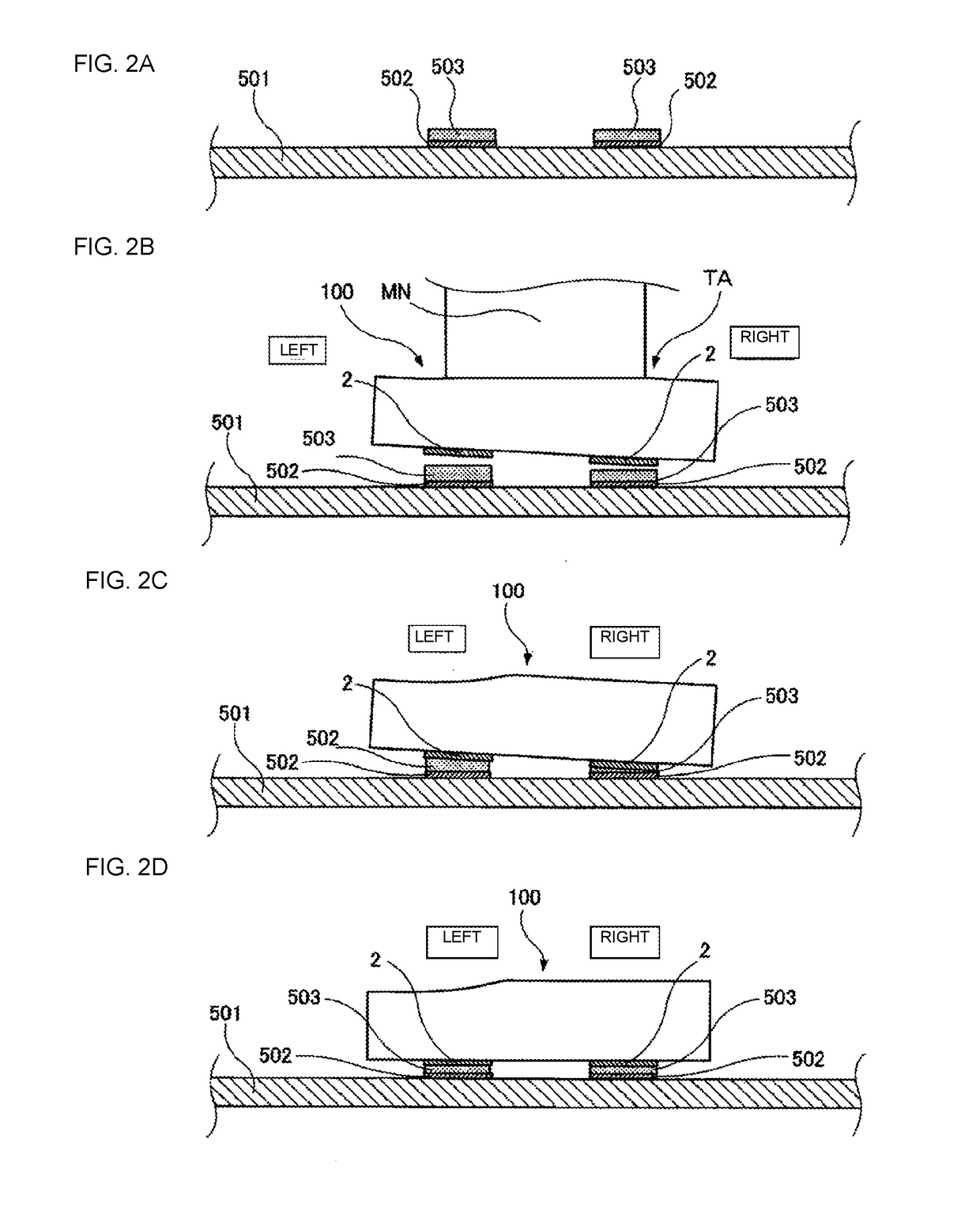
[0095]FIGS. 3A to 3C illustrate an electronic component device 200 according to a second preferred embodiment of the present invention. FIG. 3A is a sectional view of the electronic component device 200. FIG. 3B is a plan view of the electronic component device 200, and also shows in perspective built-in substrate components 6. FIG. 3C is also a plan view of the electronic component device 100, and also shows in perspective signal outer electrodes 2S and ground outer electrodes 2G that are provided on a lower principal surface. The sectional view of FIG. 3A shows a portion taken along a dash-dot line X-X in each of FIGS. 3B and 3C.

[0096]The electronic component device 200 is preferably a surface acoustic wave device, for example.

[0097]The electronic component device 200 includes a mount substrate 1.

[0098]The signal outer electrodes 2S and the ground outer electrodes 2G are provided on the lower principal surface of the mount substrate 1. Via conductors 3 and interlayer conductors 4 ...

third preferred embodiment

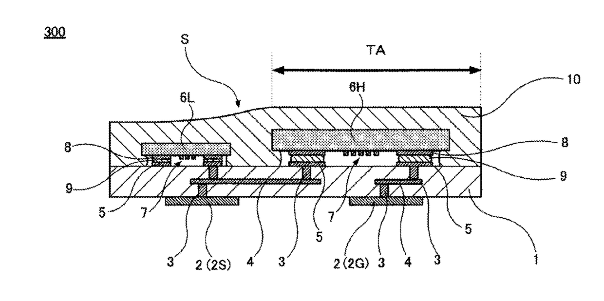
[0109]FIG. 4 illustrates an electronic component device 300 according to a third preferred embodiment of the present invention. FIG. 4 is a sectional view of the electronic component device 300.

[0110]The electronic component device 300 is an electronic component device in which changes have been made in the electronic component device 100 according to the first preferred embodiment or in the electronic component device 200 according to the second preferred embodiment.

[0111]That is, in the electronic component devices 100 or 200, two substrate components 6 with the same height or substantially the same height are built in the sealing resin layer 10. In the electronic component device 300, in place of two such substrate components 6, two substrate components 6H with a large height and two substrate components 6L with a small height are built in the sealing resin layer 10. FIG. 4 is a sectional view of one substrate component 6H with a large height and one substrate component 6L with a...


PUM


Abstract

An electronic component device includes a mount substrate including an outer electrode on one principal surface and a mount electrode on another principal surface, at least one substrate component including a terminal electrode on one principal surface, and that is mounted on the mount substrate by joining the terminal electrode to the mount electrode, and a sealing resin layer that is provided on the mount substrate on which the at least one substrate component is mounted. The sealing resin layer includes a region with a large thickness, and a top surface including an inclination.

Description

CROSS REFERENCE TO RELATED APPLICATIONS[0001]This application claims the benefit of priority to Japanese Patent Application No. 2016-129365 filed on Jun. 29, 2016. The entire contents of this application are hereby incorporated herein by reference.BACKGROUND OF THE INVENTION1. Field of the Invention[0002]The present invention relates to an electronic component device, and, more particularly, to an electronic component device that is capable of being reliably mounted on, for example, a circuit board without connection failure.[0003]In addition, the present invention relates to a method of mounting an electronic component device on a circuit board, and, more particularly, to a method of mounting an electronic component device on a circuit board, which makes it possible to reliably mount the electronic component device on the circuit board without connection failure.[0004]Further, the present invention relates to a mounting structure of an electronic component device on a circuit board...

Claims


Application Information

Patent Timeline
IPC IPC(8): H01L23/538H05K7/10H01L23/525H05K3/30H05K1/18H05K3/34H01L23/31
CPCH01L23/5389H01L23/3107H05K1/184H05K3/301H05K2201/09827H05K7/1053H05K3/3405H01L23/525H05K3/3447H01L2924/181H05K1/141H05K3/3436H01L2224/16225H01L2224/32225H01L2224/73204H01L2924/1815H05K2201/10378H05K2201/10734H01L23/3121H03H9/059H03H9/1085Y02P70/50H01L2924/00012H01L2924/00H01L23/29H03H3/08H03H9/02H03H9/17H03H9/25
Inventor WATANABE, KAZUSHI
Owner MURATA MFG CO LTD
Why Eureka
Try Eureka