Semiconductor device, electronic device, and manufacturing method
Active Publication Date: 2018-06-14
SONY CORP
View PDF13 Cites 5 Cited by
Summary
Abstract
Description
Claims
Application Information
AI Technical Summary
This helps you quickly interpret patents by identifying the three key elements:
Problems solved by technology
Method used
Benefits of technology
Benefits of technology
The patent text states that the technology helps to improve the reliability of mounting an underfill.
Problems solved by technology
The UF resin usually creeps up the side surface of the chip, and therefore there has been a concern that damage to the chip end is caused.
Method used
Image
Click on the blue label to locate the original text in one second.
Reading with bidirectional positioning of images and text.
Examples
first embodiment
1. First Embodiment
Example of Rough Configuration of Solid-State Imaging Sensor
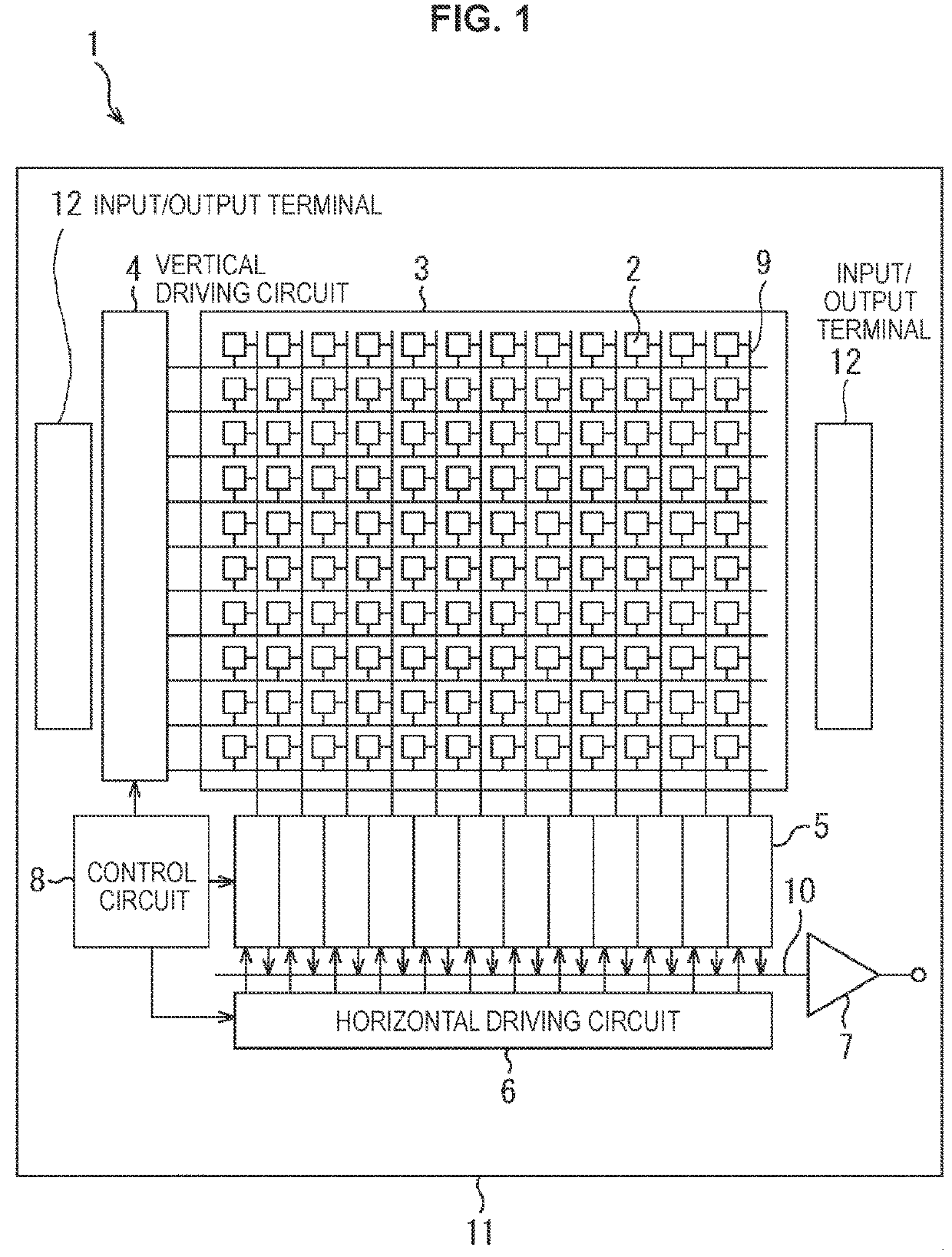
[0057]FIG. 1 shows an example of the rough configuration of an example of a complementary metaloxide semiconductor (CMOS) solid-state imaging sensor used in each embodiment of the present technology.
[0058]As shown in FIG. 1, a solid-state imaging sensor (element chip) 1 is configured to include a pixel area (what is called an imaging area) 3 in which a plurality of pixels 2 including a photoelectric conversion element are two-dimensionally arranged in a regular manner on a semiconductor substrate 11 (for example, a silicon substrate) and a peripheral circuit unit.
[0059]The pixel 2 includes a photoelectric conversion element (for example, a photodiode) and a plurality of pixel transistors (what is called MOS transistors). The plurality of pixel transistors may be configured with, for example, three transistors of a transfer transistor, a reset transistor, and an amplification transistor, or may be configu...
second embodiment
2. Second Embodiment
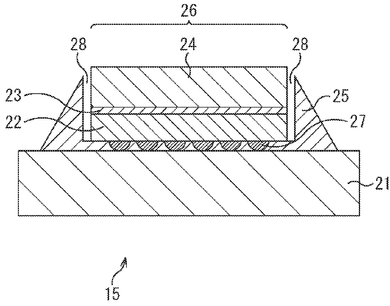
[0101]FIG. 13 is cross-sectional views showing an example of the structure of a chip scale package (CPS) of an imaging element of the present technology.
[0102]In a CPS 111 of the example of FIG. 13, a chip 120 is mounted on a mounting substrate 126 by solder balls 124, and then an underfill 125 is put between the chip 120 and the mounting substrate 126.
[0103]The chip 120 is formed by a glass substrate 122 being produced on a bonding resin 123 formed on an imaging element 121.
[0104]As shown by the tip of the arrow, the imaging element 121 is configured with a Si substrate 131 in which a circuit of an imaging element is formed, an insulating film 132, and an insulating film 133 formed after reinterconnection formation in this order from the top, and a concavity 134 is formed on an end surface (a side wall) of the insulating film 133 in a direction parallel to the upper and lower surfaces of the chip 120.
[0105]By this structure, the height of the underfill 125 is no...
third embodiment (
3. Third Embodiment (Usage Examples of Image Sensor)
[0153]FIG. 30 illustrates the usage examples of the above-described solid-state imaging sensor.
[0154]The above-described solid-state imaging sensor (image sensor) can be used for, for example, various cases in which light such as visible light, infrared light, ultraviolet light, or X-rays is detected as follows.[0155]Devices that take images used for viewing, such as a digital camera and a portable appliance with a camera function.[0156]Devices used for traffic, such as an in-vehicle sensor that takes images of the front and the back of a car, surroundings, the inside of the car, and the like, a monitoring camera that monitors travelling vehicles and roads, and a distance sensor that measures distances between vehicles and the like, which are used for safe driving (e.g., automatic stop), recognition of the condition of a driver, and the like.[0157]Devices used for home electrical appliances, such as a TV, a refrigerator, and an air...
PUM
Abstract
The present disclosure relates to a semiconductor device, an electronic device, and a manufacturing method that can maintain the mounting reliability of an underfill. A chip is formed by a circuit of an imaging element being produced on a Si substrate that is a first substrate and a second substrate being produced on an adhesive formed on the circuit. In this event, a photosensitive material is formed around the chip after the chip is mounted on a mounting substrate by a solder ball or in the state of the chip, then an underfill is formed, and then only the photosensitive material is dissolved. The present disclosure can be applied to, for example, a CMOSsolid-state imaging sensor used for an imaging device such as a camera.
Description
TECHNICAL FIELD[0001]The present disclosure relates to a semiconductor device, an electronic device, and a manufacturing method, and relates particularly to a semiconductor device, an electronic device, and a manufacturing method that can maintain the mounting reliability of an underfill.BACKGROUND ART[0002]In the mounting process of a flip chip, an underfill resin (UF resin) is put between a chip and a substrate in order to improve mounting reliability. The UF resin usually creeps up the side surface of the chip, and therefore there has been a concern that damage to the chip end is caused.[0003]Thus, the damage to the chip end has so far been prevented by adding an elastic body to the side surface to adjust stress (see Patent Literature 1).CITATION LISTPatent Literature[0004]Patent Literature 1: JP 2002-141444ADISCLOSURE OF INVENTIONTechnical Problem[0005]However, in a chip sizepackage (CSP) of a CMOSimage sensor (CIS), for example, glass and Si bonded together by a resin appear ...
Claims
Application Information
Patent Timeline
Application Date:The date an application was filed.
Publication Date:The date a patent or application was officially published.
First Publication Date:The earliest publication date of a patent with the same application number.
Issue Date:Publication date of the patent grant document.
PCT Entry Date:The Entry date of PCT National Phase.
Estimated Expiry Date:The statutory expiry date of a patent right according to the Patent Law, and it is the longest term of protection that the patent right can achieve without the termination of the patent right due to other reasons(Term extension factor has been taken into account ).
Invalid Date:Actual expiry date is based on effective date or publication date of legal transaction data of invalid patent.

