Subtractive vfet process flow with replacement metal gate and metallic source/drain

a technology of metal gate and process flow, applied in the direction of semiconductor devices, electrical devices, transistors, etc., can solve the problems of finned epitaxy having such problems, type of process flow posing a defectivity risk, and limited improvements in the manufacture of such devices

Active Publication Date: 2018-01-04
IBM CORP
View PDF4 Cites 41 Cited by
  • Summary
  • Abstract
  • Description
  • Claims
  • Application Information

AI Technical Summary

Problems solved by technology

The use of VFETs (Vertical Field-Effect Transistor) has increased over the years, but the manufacture of such devices has made limited improvements.
This type of process flow poses a defectivity risk for the finned epitaxy, at the interface between the finned epitaxy region and the bottom source / drain region upon which this epitaxy is grown.
The grown fin has such problems and others.
Such techniques also require additional gate etching (which would compromise gate resistance), but this approach poses a risk for defective epitaxial growth for the finned channel regions.
Additionally, this type of approach requires added complexity in order to form EG (thick gate dielectric) and SG (thin gate or single gate dielectric) devices.

Method used


Image

  • Subtractive vfet process flow with replacement metal gate and metallic source/drain
  • Subtractive vfet process flow with replacement metal gate and metallic source/drain
  • Subtractive vfet process flow with replacement metal gate and metallic source/drain

Examples


Embodiment Construction

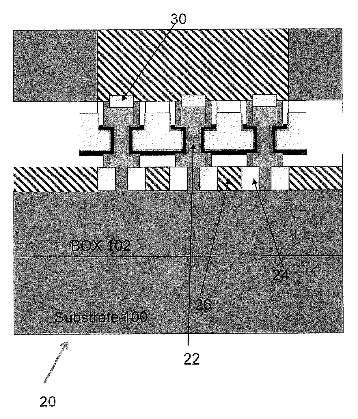
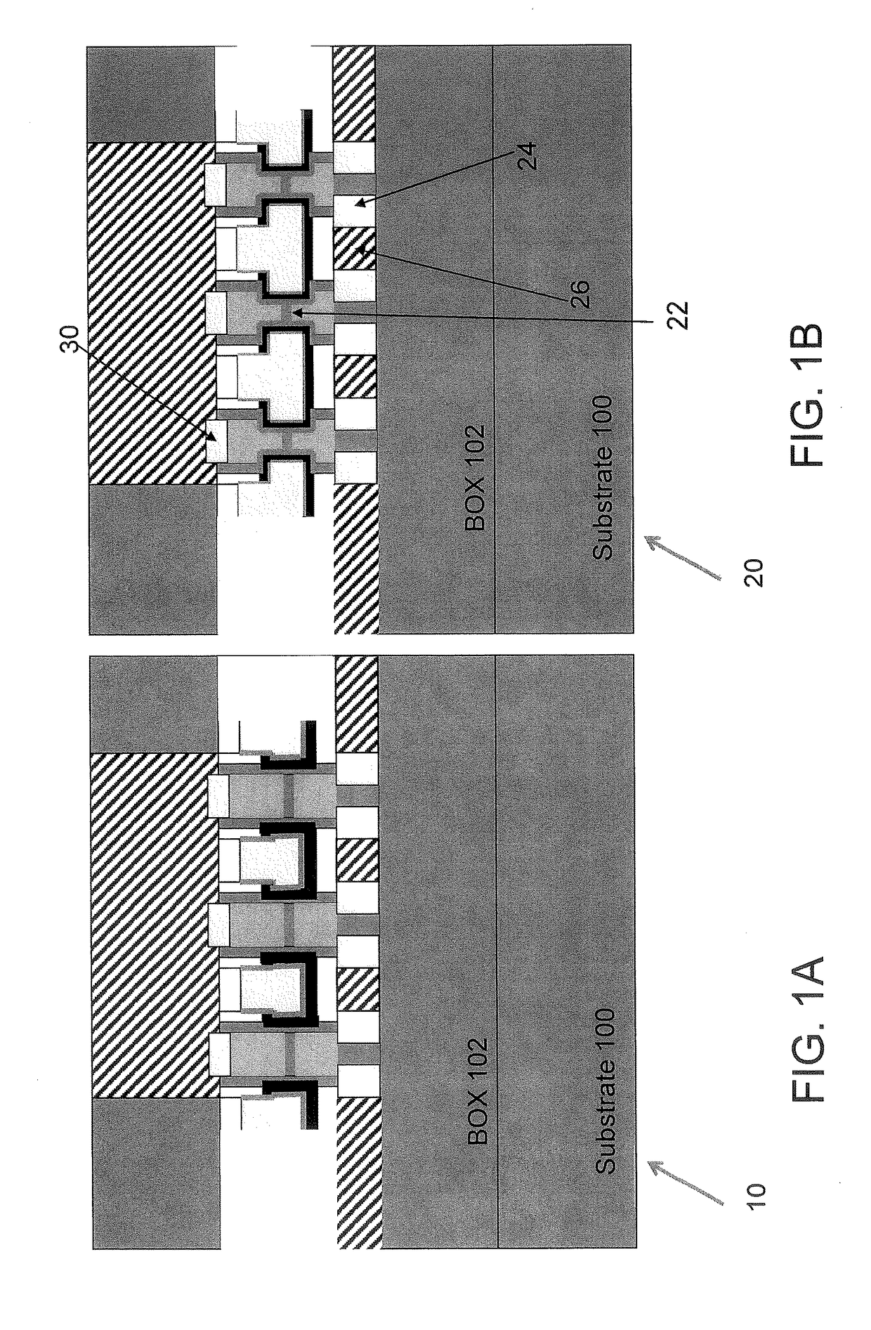
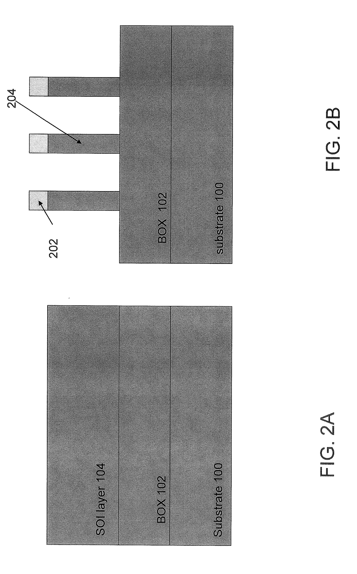
[0037]The invention will now be described with reference to the drawing figures, in which like reference numerals refer to like parts throughout. It is emphasized that, according to common practice, the various features of the drawing are not necessary to scale. On the contrary, the dimensions of the various features can be arbitrarily expanded or reduced for clarity. Exemplary embodiments are provided below for illustration purposes and do not limit the claims.

[0038]One of the problems solved by present invention is forming a VFET structure without requiring the finned channel region to be formed by growth inside a confined cavity. The present invention teaches a “subtractive” process flow, to form a VFET structure, wherein the bottom source / drain, gate, and top source / drain are all formed around an etched fin as opposed to a grown fin. The present invention furthermore teaches the formation of top and bottom metallic source / drain regions in this subtractive low context, without re...


PUM


Abstract

A method and a semiconductor device includes a substrate, and a first device type formed on the substrate, the first device type including an active channel region including a first fin, the first fin including a first fin width which is narrower than a second fin width above and below the active channel region. A second device type can be formed on the same substrate, the second device type includes a second active channel region including a second fin, the second fin including a first fin width which is the same as the second fin width both above and below the second active channel region.

Description

BACKGROUND OF THE INVENTIONField Of The Invention[0001]The present invention relates generally to a method and apparatus for Subtractive VFET process flow, and more particularly, but not by way of limitation, relating to a method and apparatus for Subtractive VFET process flow with Replacement Metal Gate and Metallic Source / Drain.Description Of The Related Art[0002]The use of VFETs (Vertical Field-Effect Transistor) has increased over the years, but the manufacture of such devices has made limited improvements. Some integration techniques require the finned channel region to be formed by growth inside a confined cavity. Such VFET integration schemes assume that the fin region is formed inside such a cavity, which is defined / etched through the material that eventually becomes the bottom source / drain spacer. This type of process flow poses a defectivity risk for the finned epitaxy, at the interface between the finned epitaxy region and the bottom source / drain region upon which this ep...

Claims


Application Information

Patent Timeline
Patent Type & Authority Applications(United States)
IPC IPC(8): H01L29/10H01L21/8234H01L27/088H01L29/78
CPCH01L29/1037H01L21/823412H01L29/7827H01L27/088H01L21/823487H01L29/0847H01L29/41741H01L29/665H01L29/66545H01L29/66666H01L29/78642
Inventor MALLELA, HARI V.ROBISON, ROBERT RUSSELLVEGA, REINALDO ARIELVENIGALLA, RAJASEKHAR
Owner IBM CORP
Why Eureka
Try Eureka