Pixel structure, display apparatus including the pixel structure, and method of manufacturing the pixel structure

Active Publication Date: 2018-01-11
SAMSUNG DISPLAY CO LTD
View PDF4 Cites 40 Cited by
  • Summary
  • Abstract
  • Description
  • Claims
  • Application Information

AI Technical Summary

Benefits of technology

[0005]One or more embodiments include pixel structures configured to prevent damage to an ultra small light-emitting diode in a process of aligning the ultra small light-emitting diode and to incr

Problems solved by technology

However, this connection may be difficult when the LED is an ultr

Method used


Image

  • Pixel structure, display apparatus including the pixel structure, and method of manufacturing the pixel structure
  • Pixel structure, display apparatus including the pixel structure, and method of manufacturing the pixel structure
  • Pixel structure, display apparatus including the pixel structure, and method of manufacturing the pixel structure

Examples


Example

COMPARATIVE EXAMPLE 1

[0077]In Comparative Example 1, the distance between the first electrode 11 and the second electrode 12 is less than a length of the ultra small light-emitting diode 30. Thus, both ends of the ultra small light-emitting diode 30 are supported by the first and second electrodes 11 and 12. The first contact electrode 51 may be connected to the first electrode 11 and the ultra small light-emitting diode 30 and the second contact electrode 52 may be connected to the ultra small light-emitting diode 30 and the second electrode 12.

Example

Embodiment 1

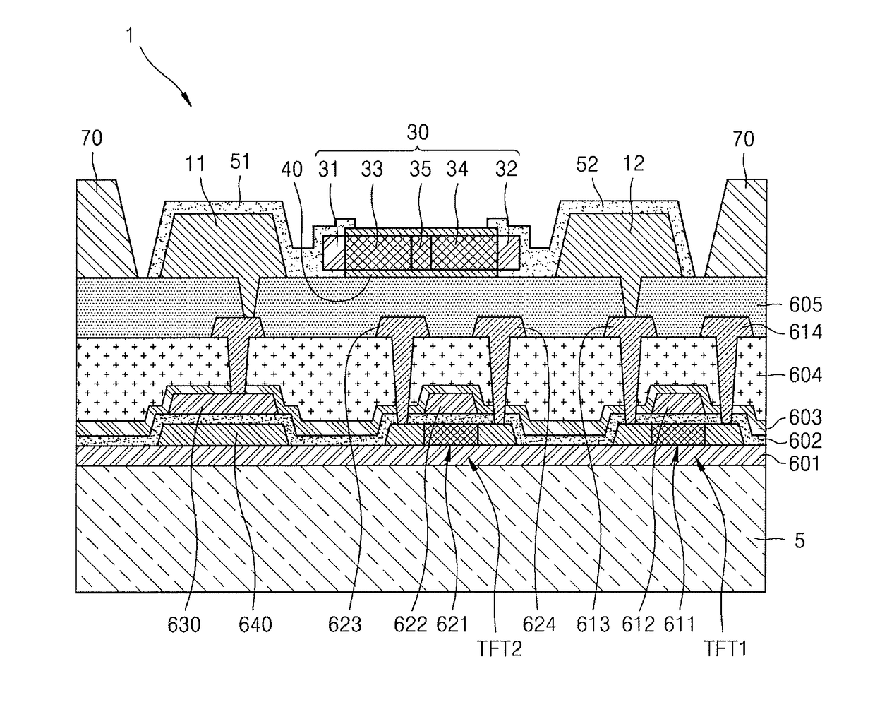
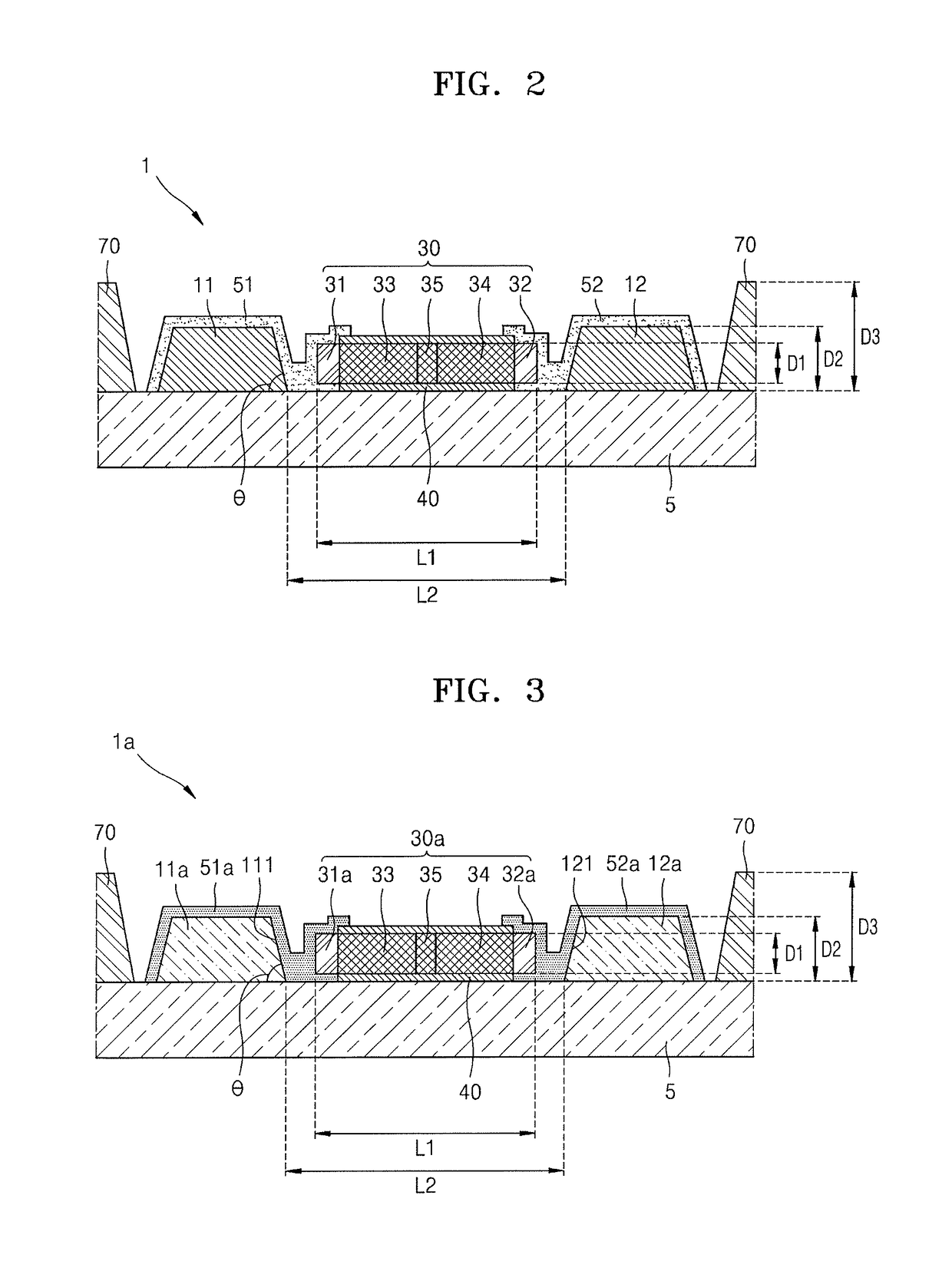
[0078]The pixel structure 1 according to Embodiment 1 is illustrated in FIG. 3. In Embodiment 1, the distance L2 between the first and second electrodes 11a and 12a is greater than the length L1 of the ultra small light-emitting diode 30a. Thus, both ends of the ultra small light-emitting diode 30a may not directly contact the first and second electrodes 11a and 12a. The first electrode 11a and the ultra small light-emitting diode 30a are connected by the transparent first contact electrode 51a, and the second electrode 12a and the ultra small light-emitting diode 30a are connected by the transparent second contact electrode 52a. The first and second electrode layers 31a and 32a of the ultra small light-emitting diode 30a are transparent electrodes.

[0079]In the first and second electrodes 11a and 12a, surface facing the ultra small light-emitting diode 30a are reflection surfaces 111 and 121. An angle of the reflection surfaces 111 and 121 with respect to the base substr...

Example

Embodiment 2

[0080]The pixel structure 1d according to the Embodiment 2 is illustrated in FIG. 7. In Embodiment 2, the distance L2 between the first and second electrodes 11a and 12a is greater than the length L1 of the ultra small light-emitting diode 30a. Thus, the both ends of the ultra small light-emitting diode 30a may not directly contact the first and second electrodes 11a and 12a. The reflection plate 80 is formed in the base substrate 5.

[0081]An example of light extraction efficiencies of the Comparative example 1 and Embodiments 1 and 2 is set forth in Table 1.

TABLE 1ComparativeEmbodiment Embodiment ItemsExample 112Emission efficiency7.4%18.5%24%

[0082]Referring to Table 1, Comparative example 1, Embodiment 1, and Embodiment 2 respectively have light extraction efficiencies of 7.4%, 18.5%, and 24%. Thus, the emission efficiency of Embodiment 1 is 250% higher than Comparative Example 1, and the emission efficiency of Embodiment 2 is 324% higher than Comparative Example 1.

[008...


PUM


Abstract

A pixel structure of a display apparatus includes an electrode line, at least one ultra small light-emitting diode, and a connection electrode. The electrode line includes a second electrode separated from a first electrode and at a same level as the first electrode on a base substrate. The at least one ultra small light-emitting diode is on the base substrate and has a length less than a distance between the first and second electrodes. A connection electrode includes a first contact electrode connecting the first electrode to the ultra small light-emitting diode and a second contact electrode connecting the second electrode to the ultra small light-emitting diode.

Description

CROSS-REFERENCE TO RELATED APPLICATION[0001]Korean Patent Application No. 10-2016-0087384, filed on Jul. 11, 2016, and entitled: “Pixel Structure, Display Apparatus Including the Pixel Structure, and Method of Manufacturing the Pixel Structure,” is incorporated by reference herein in its entirety.BACKGROUND1. Field[0002]One or more embodiments described herein relate to a pixel structure, a display apparatus including a pixel structures, and a method for manufacturing a pixel structure.2. Description of the Related Art[0003]A light-emitting diode (LED) has high optical conversion efficiency, very low power consumption, a semi-permanent lifetime, and is eco-friendly device. Accordingly, LEDs are used for traffic lights, mobile phones, headlights of vehicles, outdoor electronic displays, back light units, indoor illuminations, and other applications.[0004]When used in a display, an LED is connected to an electrode to receive supply power. In establishing this connection, attempts have...

Claims


Application Information

Patent Timeline
IPC IPC(8): H01L25/16H01L25/075H01L27/12H01L33/60H01L33/42H01L33/32H01L33/62H01L21/68H01L33/06
CPCH01L25/167H01L33/60H01L33/325H01L33/62H01L21/68H01L25/0753H01L27/124H01L2933/0066H01L33/06H01L33/42G09F9/33H01L2224/95085H05B33/12H05B33/10H05B33/20H01L27/1214H01L33/00H01L2924/12041H01L33/385H01L33/387
Inventor KIM, DAEHYUNIM, HYUNDEOKCHO, HYUNMINKANG, JONGHYUKHONG, SUNGJINLEE, JOOYEOLCHO, CHIO
Owner SAMSUNG DISPLAY CO LTD
Why Eureka
Try Eureka