
Method For Calibrating Brightness Unevenness Of OLED Display Panel

a technology of brightness unevenness and display panel, which is applied in the direction of cathode-ray tube indicators, static indicating devices, instruments, etc., can solve the problems of large mura area, inefficient method, and deviation of the gamma curve of each pixel of the oled panel, so as to improve the accuracy of calibrating brightness and efficiency. , the effect of more accura

Active Publication Date: 2018-02-08
TCL CHINA STAR OPTOELECTRONICS TECH CO LTD
View PDF9 Cites 19 Cited by
  • Summary
  • Abstract
  • Description
  • Claims
  • Application Information

AI Technical Summary

Benefits of technology

The present patent is about a method for calibrating the brightness unevenness of OLED display panels. This method involves getting the brightness matrix of the panel at least three gray scales, identifying the uniform brightness area and the uneven brightness area, and calculating the fitting Gamma value for each pixel in the uneven brightness area based on the brightness matrix. By calibrating based on this fitting Gamma curve and value, the method is more accurate than previous methods, improving the accuracy and efficiency of calibration.

Problems solved by technology

The disadvantage of this method is, the deviation of the Gamma curve of the each pixel of the OLED panel, especially the Mura area is larger.
Because the Gamma characteristic of the Mura area is unknown, a single adjustment is often less than the desired effect, and is generally requires repeated shooting and trimming the gray scale to achieve the uniform brightness.
This method is extremely inefficient, the repeated testing is required to reach the uniform brightness.

Method used


Image

  • Method For Calibrating Brightness Unevenness Of OLED Display Panel
  • Method For Calibrating Brightness Unevenness Of OLED Display Panel
  • Method For Calibrating Brightness Unevenness Of OLED Display Panel

Examples


Embodiment Construction

[0030]With reference to the following detailed description of the present disclosure.

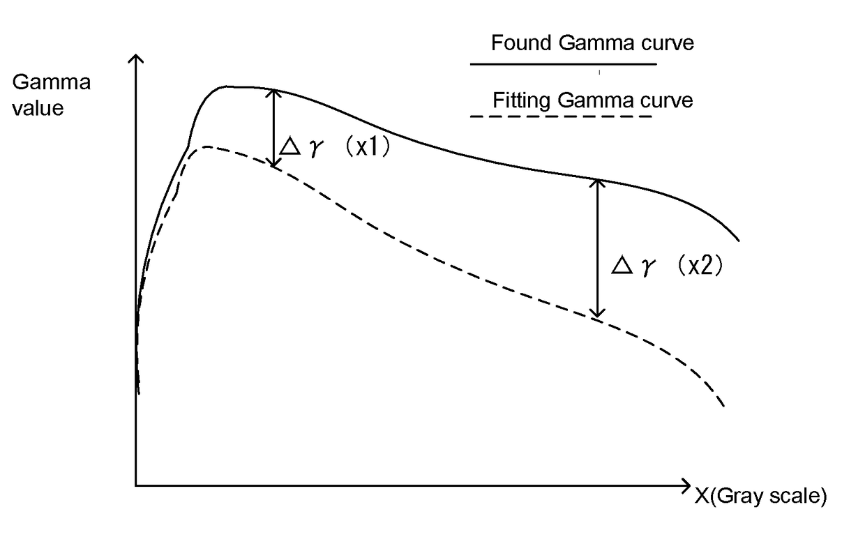
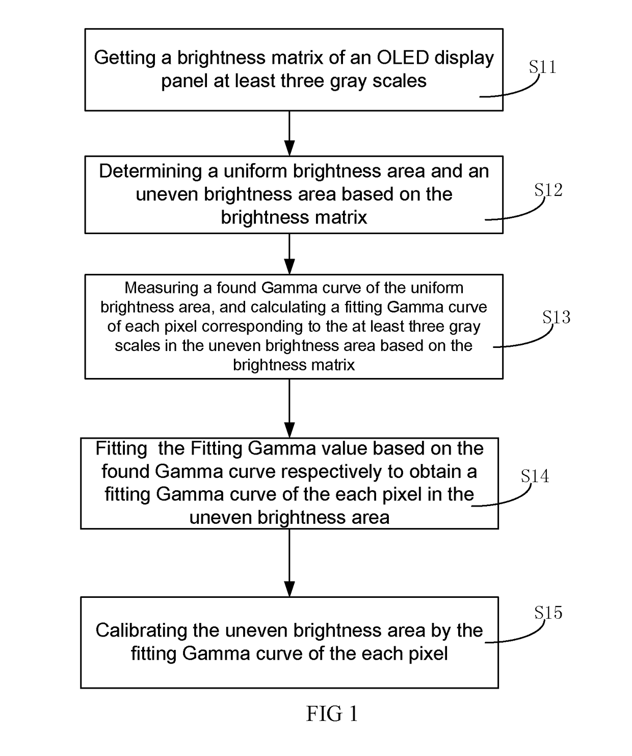
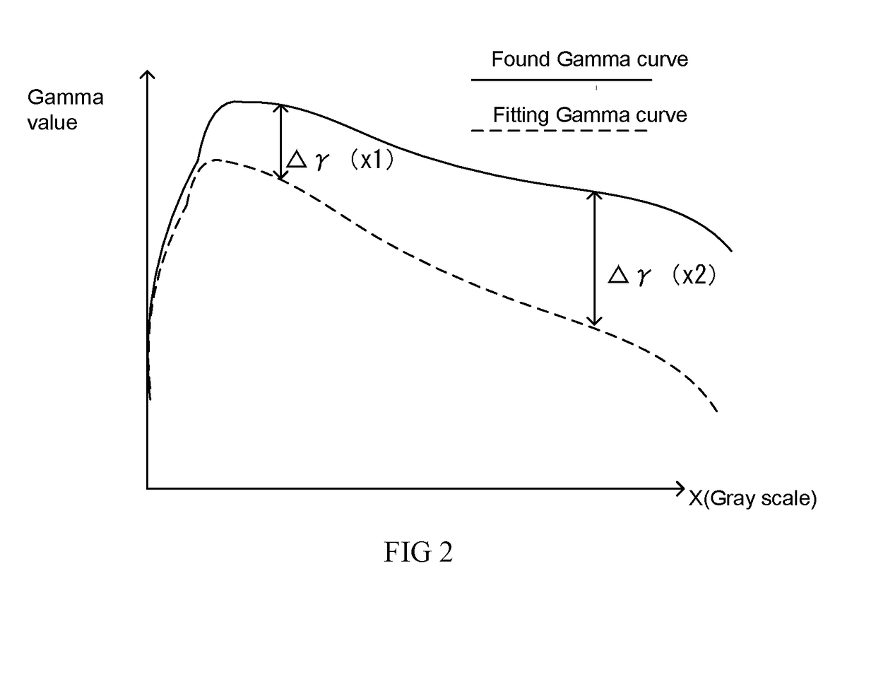
[0031]Referring to FIG. 1 and FIG. 2, FIG. 1 is a flow chart of the method for calibrating brightness unevenness of OLED display panel of the preferred embodiment of the present disclosure. FIG. 2 is a schematic diagram of the fitting Gamma curve and the found Gamma curve. The fitting Gamma curve and the found Gamma curve in the FIG. 2 are only a schematic diagram, the actual fitting Gamma curve and the actual found Gamma curve can be other shapes. In the present embodiment, the method for calibrating the brightness unevenness of the OLED display panel includes:

[0032]Step S11: getting a brightness matrix of an OLED display panel in at least three gray scales.

[0033]In the step S11: preferably, getting a brightness matrix of an OLED display panel in at least three gray scales includes: shooting in at least three gray scales, and analyzing the photos to obtain the brightness matrix corresponding to the...


PUM


Abstract

The present disclosure provides a method for calibrating brightness unevenness of an OLED display panel, the method includes: getting a brightness matrix of an OLED display panel in at least three gray scales, and determining a uniform brightness area and an uneven brightness area, and calculating a fitting Gamma value of each pixel corresponding to the at least three gray scales in the uneven brightness area, and fitting the fitting Gamma curve of the each pixel in the uneven brightness area, and calibrating the brightness of the uneven brightness area based on the fitting Gamma curve of the each pixel. The present disclosure can improve the accurate of the calibrating brightness and the efficiency of the calibration.

Description

FIELD OF THE DISCLOSURE[0001]The present disclosure relates to an OLED display technology field, and more particularly to a method for calibrating brightness unevenness of an OLED display panel.BACKGROUND OF THE DISCLOSURE[0002]The prior art of removing Mura defect of the OLED (Organic Light-Emitting Diode) panel is similar to the LCD (Liquid Crystal Display), which getting the brightness of the each pixel on the panel first, then measuring the Mura (Japanese, the term of the display technology field means uneven brightness) and setting the ideal brightness of the Mura area, finally calculating the gray scale value or the voltage value of compensating the Mura area needed based on the Gamma curve or the gray—brightness table.[0003]But the OLED is different from the LCD, the each pixel of the LCD Gamma curve is relatively consistent, the each pixel of the OLED Gamma curve is large-difference so that the OLED cannot in accordance with the unified compensation to the Mura.[0004]In the ...

Claims


Application Information

Patent Timeline
Patent Type & Authority Applications(United States)
IPC IPC(8): G09G5/10G09G3/3208G09G3/20
CPCG09G3/3208G09G2320/0285G09G2320/0673G09G3/2007G09G2320/0233G09G5/10G09G2320/0693G09G3/006
Inventor DENG, YUFAN
Owner TCL CHINA STAR OPTOELECTRONICS TECH CO LTD
Learn More