Light-emitting device (LED) and LED displaying circuit

a technology of led displaying circuit and light-emitting device, which is applied in the direction of static indicating devices, instruments, etc., can solve the problems of low luminous efficiency of sub-pixels at low driving current, unstable performance of led, and unsatisfactory relationship between luminance and driving current of led, so as to reduce the problem of color displaying and reduce the occupation area of the driving circuit for pixel

Active Publication Date: 2018-02-22
INNOLUX CORP
View PDF6 Cites 12 Cited by
  • Summary
  • Abstract
  • Description
  • Claims
  • Application Information

AI Technical Summary

Benefits of technology

[0008]Accordingly, the present invention provides the μ-LED displaying circuits, which can at least reduce the issue for color displaying at low gray level. In addition, the present invention provides the μ-LED displaying circuits which can reduce the occupation area of the driving circuit for the pixel.

Problems solved by technology

However, the relation between the luminance and the driving current of the LED is not ideally linear.
Particularly, when the driving current is low, the performance of the LED is not stable, and would have a large deviation for each sub-pixel.
Because the sub-pixels has low luminous efficiency at low driving current.
When the image resolution greatly increase, such as 4K resolution level, the driving circuit for each sub-pixel in total would consume a large circuit area.
It would cause an issue in design when the image resolution in display quality is expected be higher and higher.

Method used


Image

  • Light-emitting device (LED) and LED displaying circuit
  • Light-emitting device (LED) and LED displaying circuit
  • Light-emitting device (LED) and LED displaying circuit

Examples


Embodiment Construction

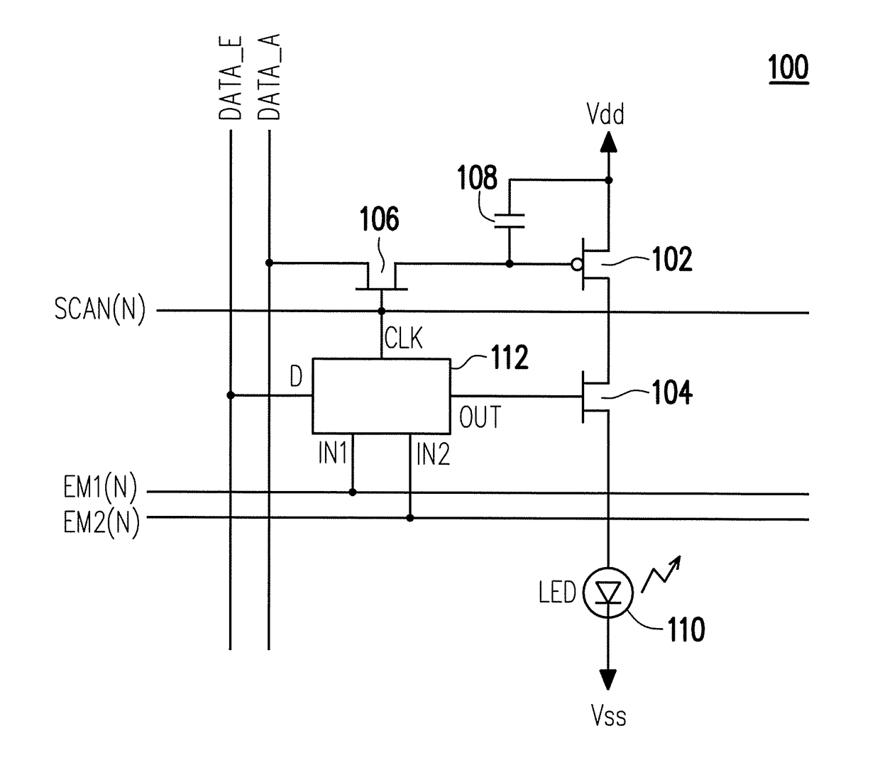
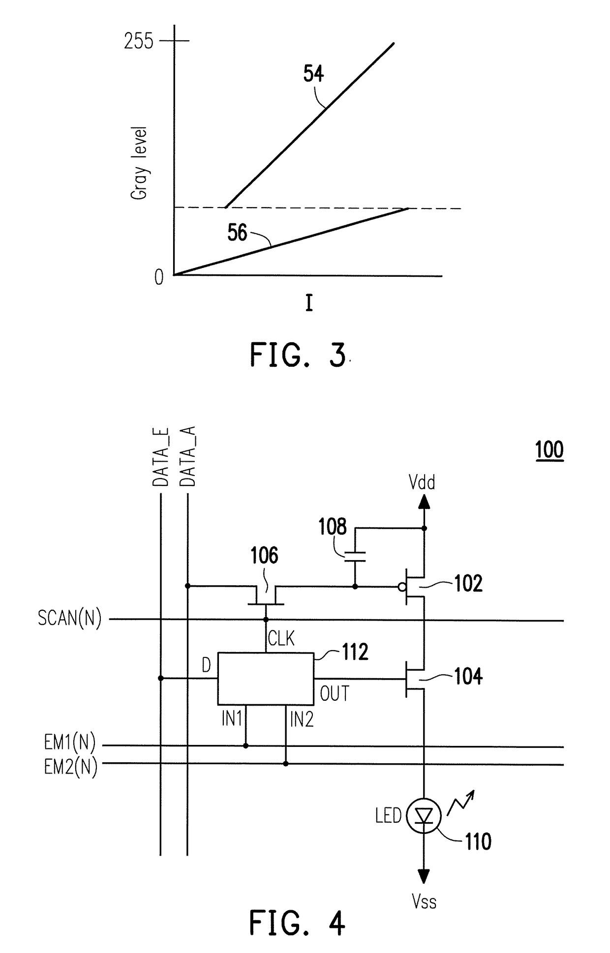
[0034]Reference will now be made in detail to the present preferred embodiments of the invention, examples of which are illustrated in the accompanying drawings.

[0035]Wherever possible, the same reference numbers are used in the drawings and the description to refer to the same or like parts.

[0036]The invention provides multiple embodiments to describe the LED displaying circuits. However, the invention about the LED displaying circuits is not limited to the embodiment as provided. Further, the embodiments as provided can be combined as well.

[0037]The LED displaying circuits can at least reduce the issue for color displaying at low gray level and also reduce the occupation area of the driving circuit for the pixel. The descriptions in better detail are provided as follows.

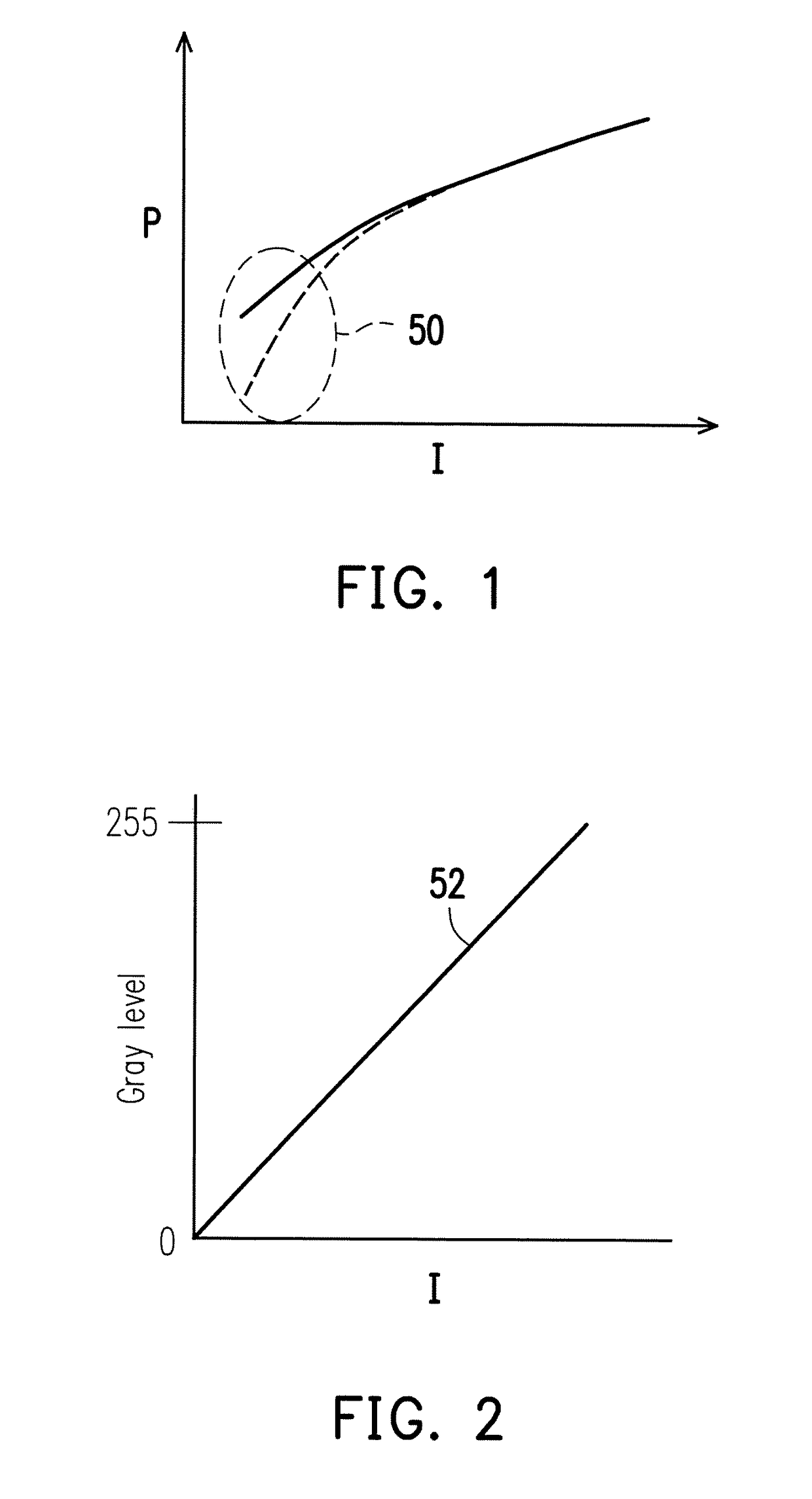
[0038]FIG. 1 is a drawing, schematically illustrating a relation between the output power (P) of LED and the driving current (I), as considered in the invention. Referring to FIG. 1, a relation between the output p...


PUM


Abstract

A light-emitting device (LED) includes a primary driving circuit and a pixel. The primary driving circuit receives a system high voltage, a data signal, and a scan signal from a scan line, wherein the primary driving circuit has an output terminal. The pixel includes a plurality of light-emitting sub-pixel circuits. Each of the light-emitting sub-pixel is coupled to the output terminal of the primary driving circuit. Wherein, a frame period includes multiple equal fields, the light-emitting sub-pixel circuits are respectively corresponding to the fields and are activated according to a sequence as assigned. The light-emitting device display includes a plurality of light-emitting sub-pixel circuits are activated in raw, in column or both according to a sequence as assigned.

Description

CROSS-REFERENCE TO RELATED APPLICATION[0001]This application claims the priority benefits of U.S. provisional application Ser. No. 62 / 376,925, filed on Aug. 19, 2016 and U.S. provisional application Ser. No. 62 / 415,542, filed on Nov. 1, 2016. The entirety of each of the above-mentioned patent applications is hereby incorporated by reference herein and made a part of this specification.BACKGROUND OF THE INVENTION1. Field of the Invention[0002]The present invention generally relates to light-emitting device (LED) display panel, in particular, to a LED displaying circuit.2. Description of Related Art[0003]As usually known, the LED such as organic LED (OLED) or micro-LED can be fabricated to emit red light, green light, or blue light, which is one of the three primary color lights. One pixel usually comprises three sub-pixels tightly put together as one pixel. The three sub-pixels respectively display the red light, green light, and blue light according to the gray levels. The primary c...

Claims


Application Information

Patent Timeline
Patent Type & Authority Applications(United States)
IPC IPC(8): G09G3/20G09G3/32
CPCG09G3/2074G09G3/32G09G2320/0666G09G2300/0452G09G2300/0842
Inventor WATSUDA, HIROFUMI
Owner INNOLUX CORP
Why Eureka
Try Eureka