Integrated sensing module, integrated sensing assembly and method of manufacturing the integrated sensing module
a sensing module and integrated sensing technology, applied in the field of integrated sensing modules, can solve the problems of increasing cost and design complexity, time-consuming and labor-intensive manufacturing process, misreading problem, etc., and achieve the effect of reducing size, easy control of quality, and standardized manufacturing process
- Summary
- Abstract
- Description
- Claims
- Application Information
AI Technical Summary
Benefits of technology
Problems solved by technology
Method used
Image

Examples
first embodiment
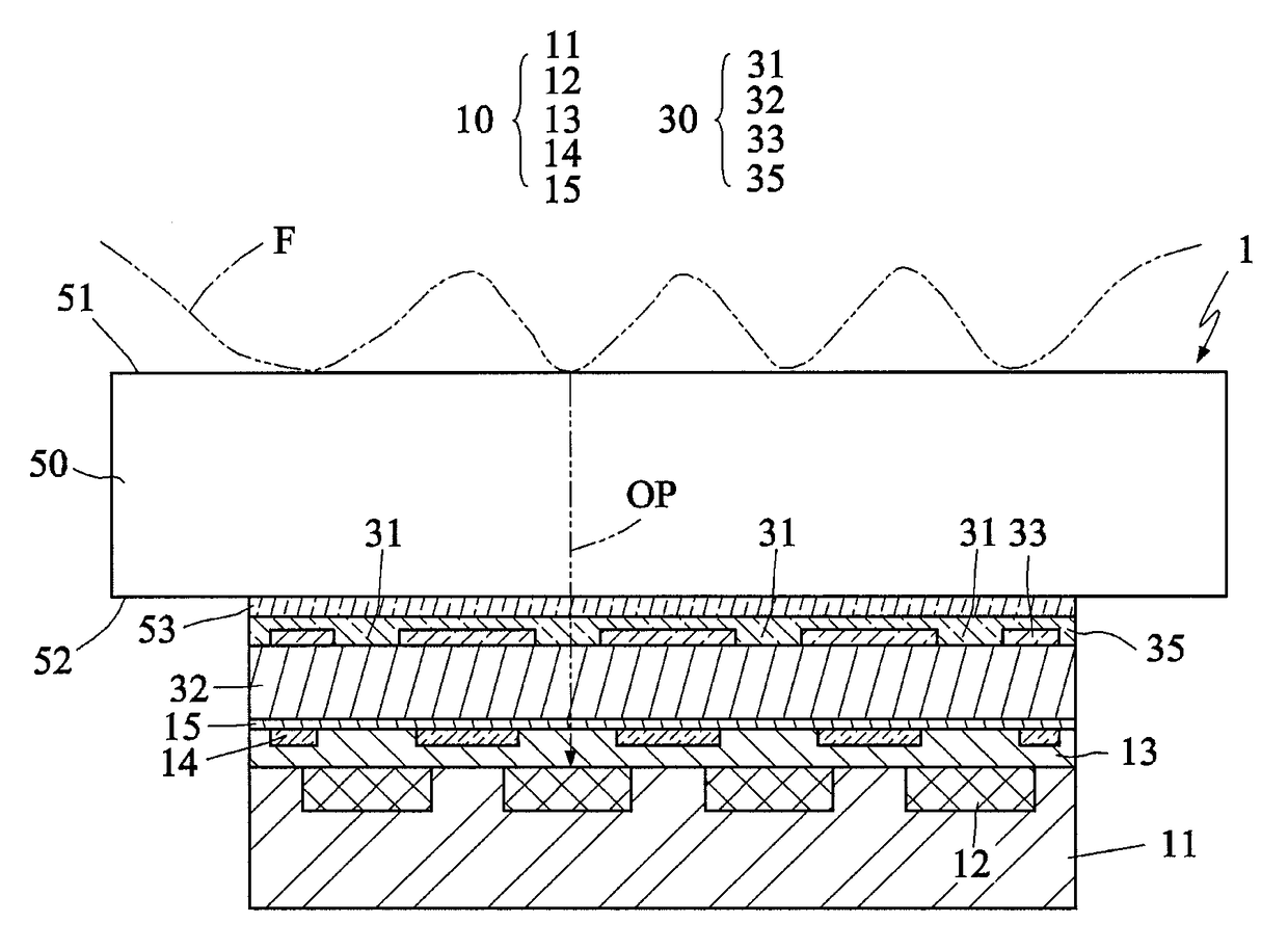
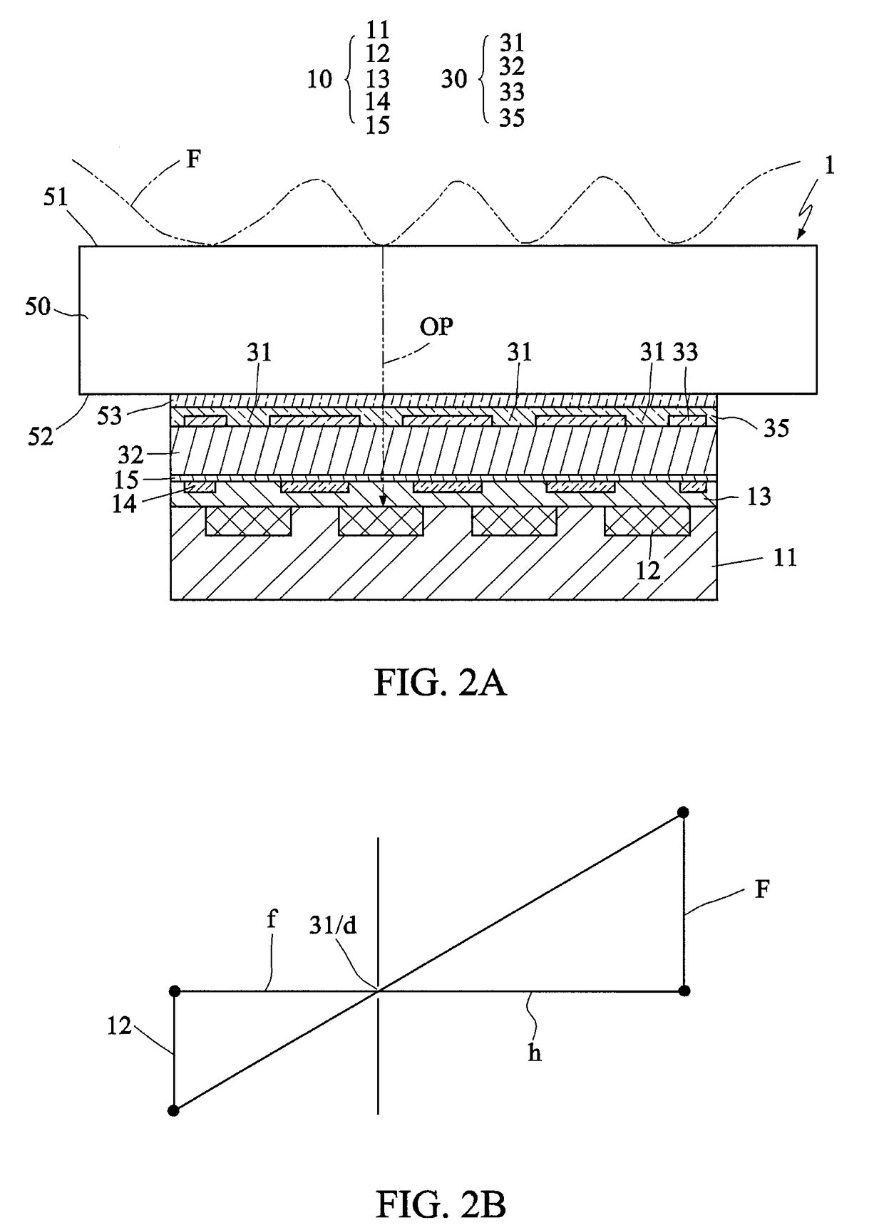
[0032]FIG. 2A is a schematic view showing an array image sensing module or an integrated sensing module 1 according to the present invention. Referring to FIG. 2A, the array image sensing module 1 includes: an image sensing chip 10, including photo sensing units 12 arranged in a two-dimensional array; and a micro-hole layer 30 disposed on the image sensing chip 10 and having multiple micro holes 31 arranged in a two-dimensional micro-hole array, the micro holes 31 corresponding to the photo sensing units 12 (may be a one-to-one, one-to-many or many-to-one geometric arrangement to match with the system design upon application without departing from the basic architecture and principles of the invention), wherein the photo sensing units 12 sense an optical image of an object F through the micro holes 31 (through the light path OP). The optical image can be a skin / dermal fingerprint image, a subcutaneous vein image and / or the array image sensing module may measure other biometrics imag...
second embodiment
[0053]The invention is directed to the wafer level manufacturing. For the sake of illustration, the schematic scale of the partial chip is described herein. First, an image sensing chip 10 is provided by, for example but without limitation to, the CMOS process for manufacturing the CMOS image sensor (CIS). FIG. 8 is a schematic view showing an integrated sensing module 1A according to the invention. Referring to FIG. 8, the integrated sensing module 1A of this embodiment includes: an image sensing chip 10 including photo sensing units 12 arranged in a two-dimensional array; a micro-hole layer 30 disposed on the image sensing chip 10 and having a micro hole 31 corresponding to the photo sensing units 12; and a transparent cover assembly 40 disposed on the micro-hole layer 30, wherein the photo sensing units 12 sense, through the micro hole 31, an optical image of an object F disposed on or over the transparent cover assembly 40.
[0054]The reason of including the transparent cover asse...
fifth embodiment
[0074]FIG. 17 shows an application of an integrated sensing module having multiple micro holes according to the invention. In this non-restrictive embodiment, four micro holes 31A to 31D are present, and correspond to four overlapping sensing ranges 12A to 12D of four sensing unit arrays. This can enlarge the sensing surface area of the integrated sensing module, and is further applicable to the under-display application of FIG. 13B. For example, if the original single micro hole corresponds to the sensing surface area of 5 mm*5 mm, then the sensing surface area can be enlarged into 10 mm*10 mm when four micro holes are adopted, and the area of the whole finger can be sensed at a time. In addition, the total light amount of all the micro holes is increased to obtain the better sensing result, wherein the false acceptance rate (FAR) and false rejection rate (FRR) thereof are further improved, and the alignment state between the finger and the integrated sensing module also needs not ...
PUM
 Abstract
Description
Claims
Application Information
 - R&D Engineer
- R&D Manager
- IP Professional
- Industry Leading Data Capabilities
- Powerful AI technology
- Patent DNA Extraction
Browse by: Latest US Patents, China's latest patents, Technical Efficacy Thesaurus, Application Domain, Technology Topic.
© 2024 PatSnap. All rights reserved.Legal|Privacy policy|Modern Slavery Act Transparency Statement|Sitemap