Electronic circuit module

a technology of electronic circuit module and circuit, applied in the direction of printed circuit aspects, inspection/indentification of circuits, printed circuits, etc., can solve the problems of impairing shielding capability and shielding capability, and achieve superior shielding capability and excellent continuity

Active Publication Date: 2018-03-15
MURATA MFG CO LTD
View PDF11 Cites 5 Cited by
  • Summary
  • Abstract
  • Description
  • Claims
  • Application Information

AI Technical Summary

Benefits of technology

[0023]Further, since the marking has a protruding shape, the conductive film covering the marking has excellent continuity and does not include and discontinuities in a central portion thereof. Accordingly, superior shielding capability is obtained.

Problems solved by technology

In such a case, the marking may sometimes penetrate through thinner portions of the conductive film 309, and this may impair shielding capability.
This may also impair the shielding capability.

Method used


Image

  • Electronic circuit module
  • Electronic circuit module
  • Electronic circuit module

Examples


first preferred embodiment

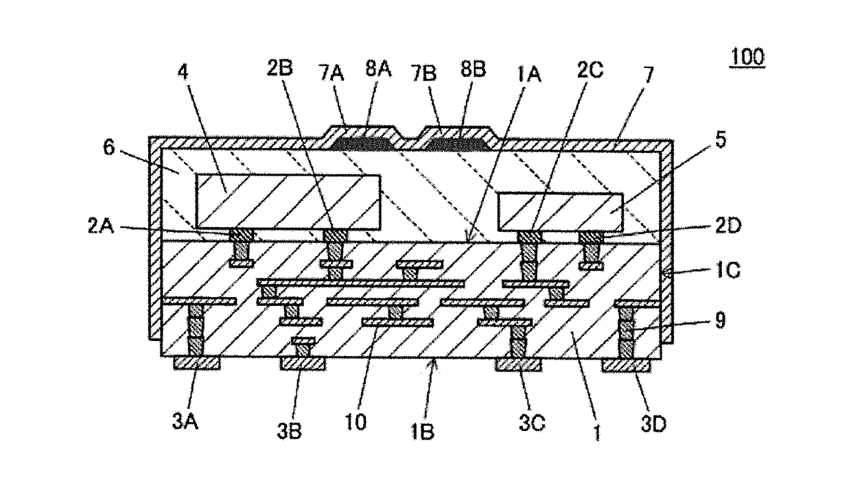
[0033]An electronic circuit module 100 that is a first preferred embodiment of an electronic circuit module according to the present invention is described with reference to FIG. 1.

[0034]FIG. 1 is a cross sectional view of the electronic circuit module 100. The electronic circuit module 100 includes a circuit board 1, electronic components 4 and 5, a burying layer 6, and a conductive film 7.

[0035]The circuit board 1 includes a first principal surface 1A on which first electrodes 2A to 2D are provided, a second principal surface 1B on which second electrodes 3A to 3D including grounding electrodes 3A and 3D are provided, and a side surface 1C connecting the first principal surface 1A and the second principal surface 1B. Further, the circuit board 1 includes internal conductors including via conductors 9 and pattern conductors 10. As the circuit board 1, it is preferable to use a multilayer substrate made of a matrix including a glass fiber enforced insulating resin material or a cera...

second preferred embodiment

[0054]An electronic circuit module 200 that is a second preferred embodiment of electronic circuit module according to the present invention is described with reference to FIG. 5.

[0055]As to duplicate elements of the electronic circuit module 100 illustrated in FIG. 1, a description thereof is omitted if appropriate.

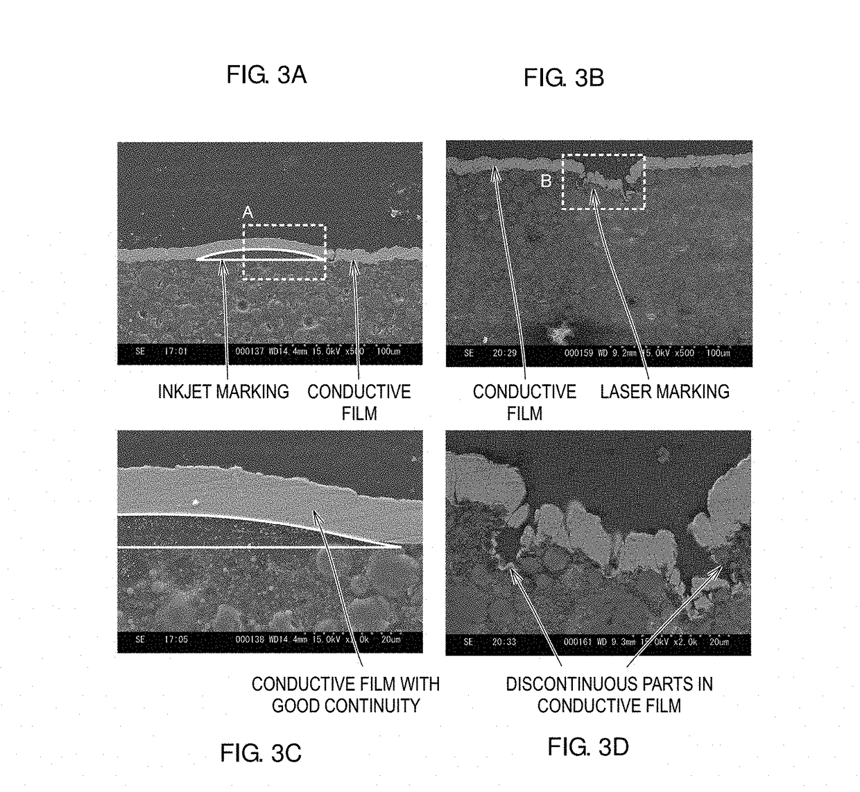
[0056]FIG. 5 is a cross sectional view of the electronic circuit module 200. The electronic circuit module 200 includes conductive markings 8A and 8B provided by, for example, an ink jet device using carbon ink, and the conductive markings 8A and 8B preferably have protruding shapes with respect to the surface of the burying layer 6. Further, the markings 8A and 8B are exposed at the conductive film 7 at their top portions while maintaining contact with the conductive film 7.

[0057]In other words, in the electronic circuit module 200, the outer surface of the burying layer 6 is covered with the conductive film 7 and the conductive markings 8A and 8B. In this case, althoug...


PUM

PropertyMeasurementUnit
conductiveaaaaaaaaaa
insulatingaaaaaaaaaa
shapeaaaaaaaaaa

Abstract

An electronic circuit module includes a circuit board, electronic components, a burying layer, and a conductive film. The circuit board includes a first principal surface on which first electrodes are provided, a second principal surface on which second electrodes including grounding electrodes are provided, and a side surface connecting the first principal surface and the second principal surface. The electronic components are connected to the first electrodes. The burying layer is provided on the first principal surface of the circuit board with the electronic components buried therein. The conductive film is connected to the grounding electrodes. The outer surface of the burying layer includes markings with protruding shapes with respect to the outer surface of the burying layer. The conductive film covers the outer surface of the burying layer.

Description

CROSS REFERENCE TO RELATED APPLICATIONS[0001]This application claims the benefit of priority to Japanese Patent Application No. 2015-098664 filed on May 14, 2015 and is a Continuation Application of PCT Application No. PCT / JP2016 / 058761 filed on Mar. 18, 2016. The entire contents of each application are hereby incorporated herein by reference.BACKGROUND OF THE INVENTION1. Field of the Invention[0002]The present invention relates to electronic circuit modules each including connecting electronic components connected to a circuit board and buried in a burying layer including a surface covered with a conductive film.2. Description of the Related Art[0003]In recent years, to meet demands for higher performance and efficient manufacturing of electronic devices, it has become more popular to use electronic circuit modules each formed by connecting electronic components to a circuit board and burying the electronic components into a burying layer whose surface is coated with a conductive f...

Claims


Application Information

Patent Timeline
Patent Type & Authority Applications(United States)
IPC IPC(8): H05K1/18H05K1/02H05K1/11H05K1/03H05K1/09
CPCH05K1/182H05K1/0266H05K1/115H05K1/0298H05K1/0306H05K1/0366H05K1/09H01L23/295H01L23/3121H01L23/544H01L23/552H01L2224/16227H01L2924/15313H01L2924/19041H01L2924/19042H01L2924/19043H01L2924/19105H01L2223/54406H01L2223/54433H01L2223/54486H05K3/284H05K2201/0715H05K2201/09936
Inventor KIDOGUCHI, MITSUAKI
Owner MURATA MFG CO LTD
Why Eureka
Try Eureka