Display device and manufacturing method thereof

a technology of display panel and manufacturing method, which is applied in the manufacture of final products, solid-state devices, basic electric elements, etc., can solve the problems of difficult deformation of display device, relatively heavy glass substrate, easy to break, etc., and achieve the effect of reducing or effectively preventing the electrical characteristics of the display panel from being deteriorated, increasing the flexibility of the connection wire in the bending area of the display panel, and improving the reliability of the bending area

Active Publication Date: 2018-03-22
SAMSUNG DISPLAY CO LTD
View PDF2 Cites 24 Cited by
  • Summary
  • Abstract
  • Description
  • Claims
  • Application Information

AI Technical Summary

Benefits of technology

[0022]According to one or more exemplary embodiment, the flexibility of the connection wire in the bending area of the display panel may be increased...

Problems solved by technology

However, the glass substrate is relatively heavy and easily broken.
Further, the gla...

Method used


Image

  • Display device and manufacturing method thereof
  • Display device and manufacturing method thereof
  • Display device and manufacturing method thereof

Examples


Embodiment Construction

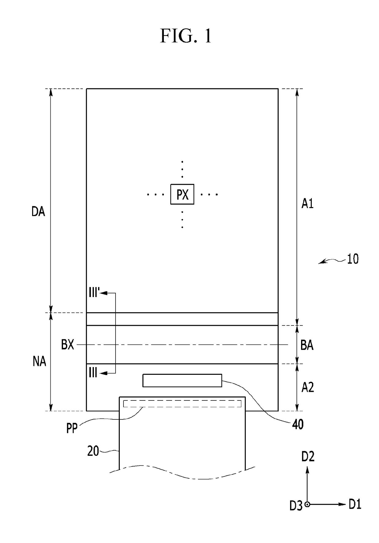
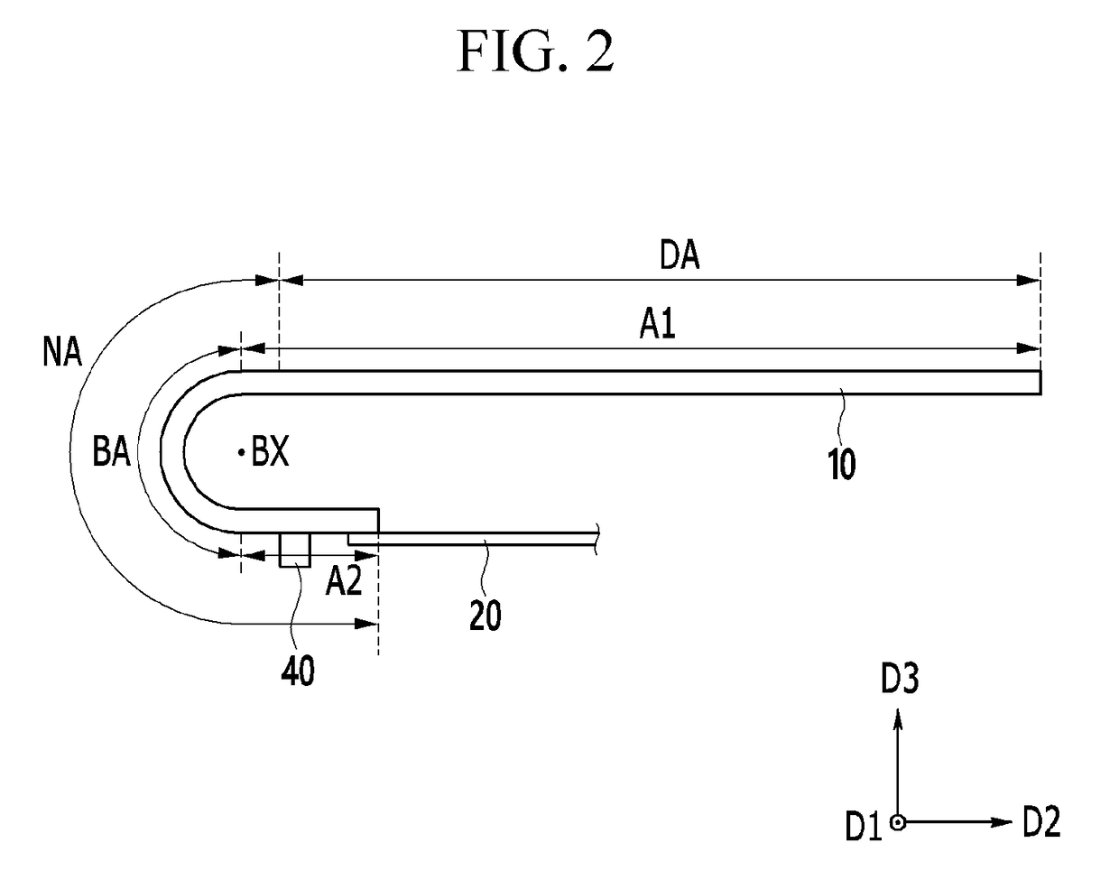
[0031]The invention will be described more fully hereinafter with reference to the accompanying drawings, in which exemplary embodiments of the invention are shown. As those skilled in the art would realize, the described embodiments may be modified in various different ways, all without departing from the spirit or scope of the invention.

[0032]The drawings and description are to be regarded as illustrative in nature and not restrictive, and like reference numerals designate like elements throughout the specification.

[0033]The size and thickness of each component shown in the drawings are arbitrarily shown for better understanding and ease of description, but the invention is not limited thereto. In the drawings, the thickness of layers, films, panels, regions, etc., are exaggerated for clarity. For better understanding and ease of description, the thickness of some layers and areas is exaggerated.

[0034]It will be understood that when an element such as a layer, film, region, or sub...


PUM


Abstract

A display device includes: a substrate including a display area, a non-display area at which the image is not displayed and a first area including the display area, the non-display area including a bending area at which the display device is bendable between the first area and a second area; a first wire in the first area, the first wire and connected to the display area; a second wire in the second area; a protection layer in the first, second and bending areas, first and second contact holes in the protection layer and exposing the first and second wires; and a connection wire connected to the first wire, extended from the first area to traverse the bending area and connected to the second wire. The connection wire includes a plurality of conductive layers contacting each other, the plurality of conductive layers including a same material.

Description

[0001]This application claims priority to Korean Patent Application No. 10-2016-0121610 filed on Sep. 22, 2016, and all the benefits accruing therefrom under 35 U.S.C. § 119, the content of which in its entirety is incorporated herein by reference.BACKGROUND(a) Field[0002]This disclosure relates to a display device and a manufacturing method thereof.(b) Description of the Related Art[0003]Display devices such as an organic light emitting device and a liquid crystal display device are manufactured by generating a plurality of layers and elements on a substrate. Glass is used for the substrate of the display device. However, the glass substrate is relatively heavy and easily broken. Further, the glass substrate is relatively rigid such that deforming the display device may be difficult. Display devices using a flexible substrate that is relatively light, strong against impacts and easily deformed have been developed.SUMMARY[0004]The invention has been made in an effort to provide a di...

Claims


Application Information

Patent Timeline
IPC IPC(8): H01L51/00H01L27/32H01L51/52
CPCH01L51/0097H01L27/3246H01L27/3276H01L27/3248H01L51/5253H01L2227/323Y02E10/549Y02P70/50H10K59/122H10K59/124H10K59/131H10K50/844H10K59/1201H10K2102/311H01L27/124H10K59/1213H10K77/111H10K71/00H10K59/123
Inventor LEE, JUNG KYUKIM, TAE HYUNPARK, SANG HOSHIM, DONG HWANLEE, SEUNG MINCHO, SEUNG-HWAN
Owner SAMSUNG DISPLAY CO LTD
Why Eureka
Try Eureka