

Charger circuit and capacitive power conversion circuit and reverse blocking switch circuit thereof
a capacitive power conversion and circuit technology, applied in the field of charger circuits, can solve the problems of inconvenient use of fast charging cables, long charging time required, and less flexibility of fast charging cables for accommodation
- Summary
- Abstract
- Description
- Claims
- Application Information
AI Technical Summary
Benefits of technology
Problems solved by technology
Method used
Image

Examples
Embodiment Construction
[0026]The drawings as referred to throughout the description of the present invention are for illustration only, to show the interrelations between the circuits and the signal waveforms, but not drawn according to actual scale.
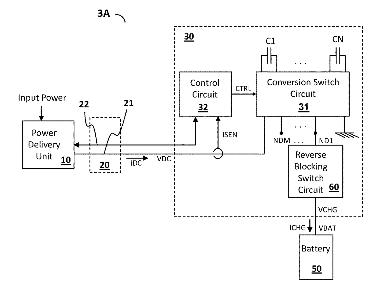
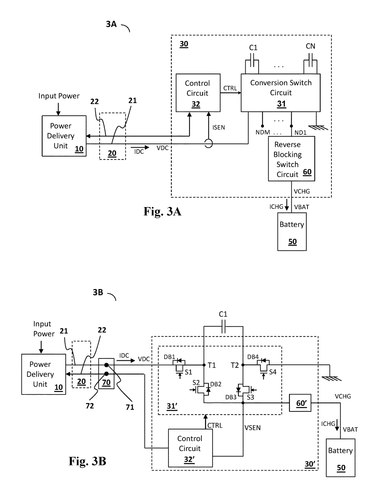
[0027]FIG. 3A shows one embodiment of the charger circuit according to the present invention (charger circuit 3A). As shown in the figure, the charger circuit 3A is configured to operably convert an input power to a DC power and convert the DC power to a charging power for charging a battery 50, wherein the DC power includes a DC voltage VDC and a DC current IDC and the charging power includes a charging voltage VCHG and a charging current ICHG. The charger circuit 3A comprises: a power delivery unit 10, and a capacitive power conversion circuit 30. The power delivery unit 10 is configured to operably convert the input power (for example but not limited to an AC power) to the DC power. The power delivery unit 10 may be for example a power adaptor which convert...
PUM
 Abstract
Description
Claims
Application Information