Image processing apparatus and method for controlling the same
- Summary
- Abstract
- Description
- Claims
- Application Information
AI Technical Summary
Benefits of technology
Problems solved by technology
Method used
Image

Examples
first embodiment
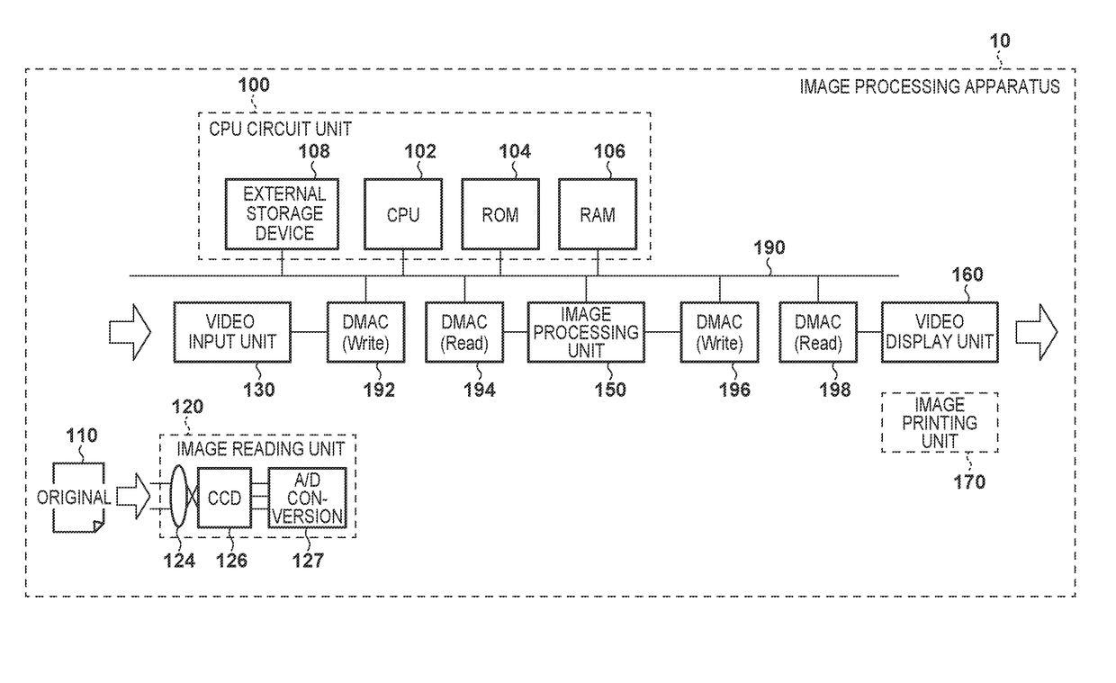
[0033]Overall Arrangement of Apparatus
[0034]FIG. 1 is a block diagram showing an example of the overall arrangement of an image processing apparatus (computer) 10 according to the first embodiment. The image processing apparatus 10 performs image processing for performing burst read-out on image data from a memory and deforming an image. The image processing apparatus 10 includes a CPU circuit unit 100, an image reading unit 120, a video input unit 130, an image processing unit 150, a video display unit 160, and an image printing unit 170. The operational overview by these components will be described below.
[0035]The image reading unit 120 includes a lens 124, a CCD sensor 126, and an analog signal processing unit 127. Image information of an original 110 is formed on the CCD sensor 126 via the lens 124. The CCD sensor 126 converts the image information into R (Red), G (Green), and B (Blue) analog electrical signals. The pieces of image information converted into the analog electric...
second embodiment
[0131]In the first embodiment, the method of performing bilinear interpolation on 2×2 pixels has been described. In the second embodiment, a bicubic pixel interpolation method using 4×4 pixels is used.
[0132]Pixel Interpolation Method (Bicubic)
[0133]In this embodiment, with respect to 16 points near four pixels in a main scanning direction×four pixels in a sub scanning direction, an interpolation coefficient of each pixel value is calculated from a coordinate fraction part of a shift amount from coordinate values at a center point, weighted interpolation is performed, and a pixel value at the center point is calculated (bicubic interpolation).
[0134]Image Format (10-Bit Y, Cb, and Cr Blocks)
[0135]The structure of image data in this embodiment will be described in detail below. FIG. 14 shows image data stored in a DRAM 106. This image data is data of 10-bit Y, Cb, Cr block formats. 10-bit luminance data “Y”, and color difference data “Cb” and “Cr” are packed in a 16-Byte (1-beat) unit....
third embodiment
[0148]In the third embodiment, extension to a raster image format of bicubic pixel interpolation will be described.
[0149]Image Format (10-Bit Y, Cb, and Cr Rasters)
[0150]The structure of image data in this embodiment will be described in detail below. FIG. 15 shows image data stored in a DRAM 106. This image data is data in 10-bit Y, Cb, and Cr raster formats. As in the second embodiment, a pixel boundary is provided in a two-pixel unit (40-bit length), and pixels are packed in the 80-Byte (5-beat) unit. Note that the raster image format is used, and thus 32×1 pixels are stored in the 80-Byte (5-beat) unit as [0, 0] to [31, 0] in FIG. 15. For example, when a transfer length is 160 Bytes (10 beats), image data of 64 pixels in the range of coordinates [0, 0] to [63, 0] is read / written per memory access.
[0151]Bank Allocation Method of Image Data on DRAM 106
[0152]A storage method and bank allocation method of image data in the DRAM 106 are basically the same as a method described in the...
PUM
 Abstract
Description
Claims
Application Information
 - R&D Engineer
- R&D Manager
- IP Professional
- Industry Leading Data Capabilities
- Powerful AI technology
- Patent DNA Extraction
Browse by: Latest US Patents, China's latest patents, Technical Efficacy Thesaurus, Application Domain, Technology Topic.
© 2024 PatSnap. All rights reserved.Legal|Privacy policy|Modern Slavery Act Transparency Statement|Sitemap