

Optoelectronic Semiconductor Chip
- Summary
- Abstract
- Description
- Claims
- Application Information
AI Technical Summary
Benefits of technology
Problems solved by technology
Method used
Image

Examples
Embodiment Construction
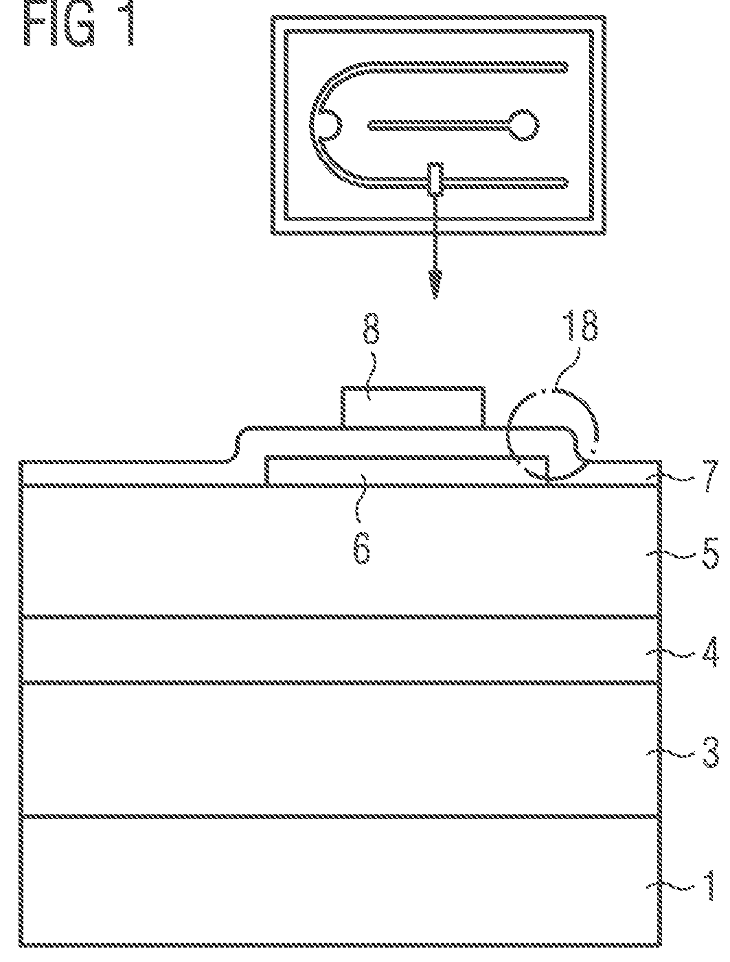
[0057]FIG. 1 shows a schematic side view and a plan view of an optoelectronic semiconductor chip according to a comparative example. The optoelectronic semiconductor chip comprises a substrate 1. An n-doped semiconductor layer 3, an active layer 4, and a p-doped semiconductor layer 5 are arranged downstream the substrate 1. A blocking element 6 is arranged downstream the p-doped semiconductor layer 5. The blocking element 6 is arranged on the radiation exit surface of the p-doped semiconductor layer 5. An electrically-conductive layer 7 is arranged downstream the blocking element 6. A p-type connection contact is arranged downstream the transparent, electrically-conductive layer 7 is. Thus, the transparent electrically-conductive layer 7 electrically connecting the p-type connection contact 8 and the p-doped semiconductor layer 5 is arranged between the p-type connection contact 8 and the p-doped semiconductor layer 5. Generally, the transparent, electrically-conductive layer 7 has ...
PUM
 Abstract
Description
Claims
Application Information