Multilayer thin-film capacitor
a multi-layer, capacitor technology, applied in the direction of capacitors, fixed capacitor details, fixed capacitors, etc., can solve the problems of reference not providing additional functions, and it is difficult to suppress noise in general multi-layer ceramic capacitors
- Summary
- Abstract
- Description
- Claims
- Application Information
AI Technical Summary
Benefits of technology
Problems solved by technology
Method used
Image

Examples
first exemplary embodiment
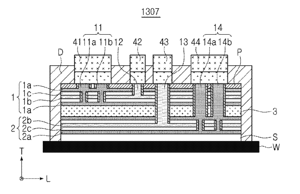
[0026]FIG. 1 is a schematic cross-sectional view illustrating a multilayer thin-film capacitor according to a first exemplary embodiment.
[0027]Referring to FIG. 1, a multilayer thin-film capacitor 100 may include a first multilayer body 1 having a structure in which dielectric layers and internal electrode layers are alternately stacked in a thickness (T) direction and a second multilayer body 2 disposed on a lower surface of the first multilayer body 1 and having a structure in which dielectric layers and internal electrode layers are alternately stacked in the thickness (T) direction. In the present disclosure, the thickness (T) direction refers to a direction in which the dielectric layers and the internal electrode layers are stacked. The first multilayer body and the second multilayer body may be stacked on each other in the same thickness (T) direction as the dielectric layers and internal electrode layers therein.
[0028]The first multilayer body 1 and the second multilayer bod...
second exemplary embodiment
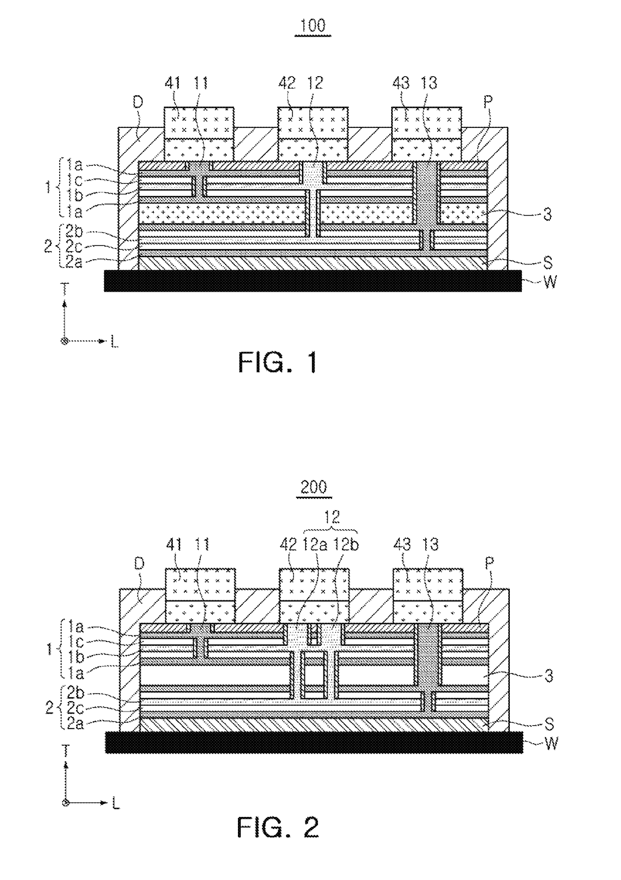
[0047]A multilayer thin-film capacitor 200 according to a second exemplary embodiment will be described with reference to FIG. 2. A description overlapping that of the multilayer thin-film capacitor according to the first exemplary embodiment will be omitted, and components substantially overlapping those of FIG. 1 will be denoted by the same reference numerals.
[0048]The multilayer thin-film capacitor 200 according to the second exemplary embodiment may include a first multilayer body 1, a second multilayer body 2 disposed below the first multilayer body 1, and a split layer 3 extending in a horizontal direction so as to separate the first and second multilayer bodies from each other in a vertical direction. A first external terminal 41, a second external terminal 42, and a third external terminal 43 may be disposed on an upper surface of the first multilayer body 1. Also in the second exemplary embodiment, the first and third external terminals 41 and 43 may constitute a signal out...
third exemplary embodiment
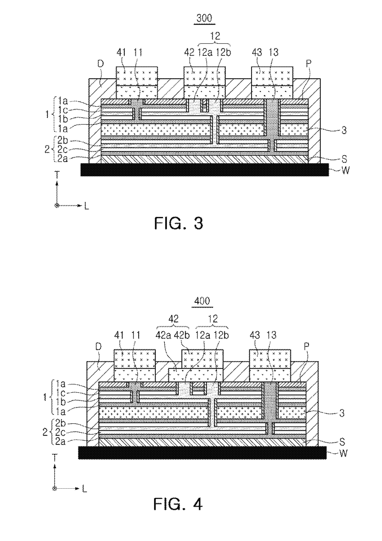
[0052]Next, a multilayer thin-film capacitor 300 according to a third exemplary embodiment will be described with reference to FIG. 3. A description overlapping that of the multilayer thin-film capacitor according to the first exemplary embodiment will be omitted, and components substantially overlapping those of FIG. 1 will be denoted by the same reference numerals.
[0053]The multilayer thin-film capacitor 300 according to the third exemplary embodiment may include a first multilayer body 1, a second multilayer body 2 disposed below the first multilayer body 1, and a split layer 3 extending in a horizontal direction so as to separate the first and second multilayer bodies from each other in a vertical direction. A first external terminal 41, a second external terminal 42, and a third external terminal 43 may be disposed on an upper surface of the first multilayer body 1. Also in the third exemplary embodiment, the first and third external terminals 41 and 43 may constitute a signal ...
PUM
 Abstract
Description
Claims
Application Information
 - R&D Engineer
- R&D Manager
- IP Professional
- Industry Leading Data Capabilities
- Powerful AI technology
- Patent DNA Extraction
Browse by: Latest US Patents, China's latest patents, Technical Efficacy Thesaurus, Application Domain, Technology Topic.
© 2024 PatSnap. All rights reserved.Legal|Privacy policy|Modern Slavery Act Transparency Statement|Sitemap