Electronics package having a multi-thickness conductor layer and method of manufacturing thereof
a technology of conductor layer and electronic package, which is applied in the direction of semiconductor devices, semiconductor/solid-state device details, electrical apparatus, etc., can solve the problems of reducing the electrical performance of the overall package, limiting the product level miniaturization, design flexibility and cost efficiency, and adding considerable thickness to the overall electronics packag
- Summary
- Abstract
- Description
- Claims
- Application Information
AI Technical Summary
Benefits of technology
Problems solved by technology
Method used
Image

Examples
Embodiment Construction
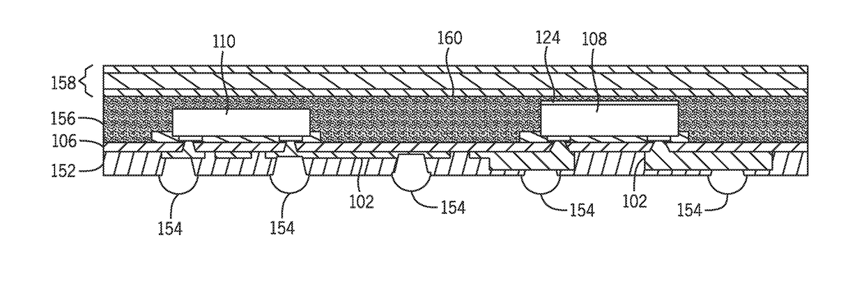
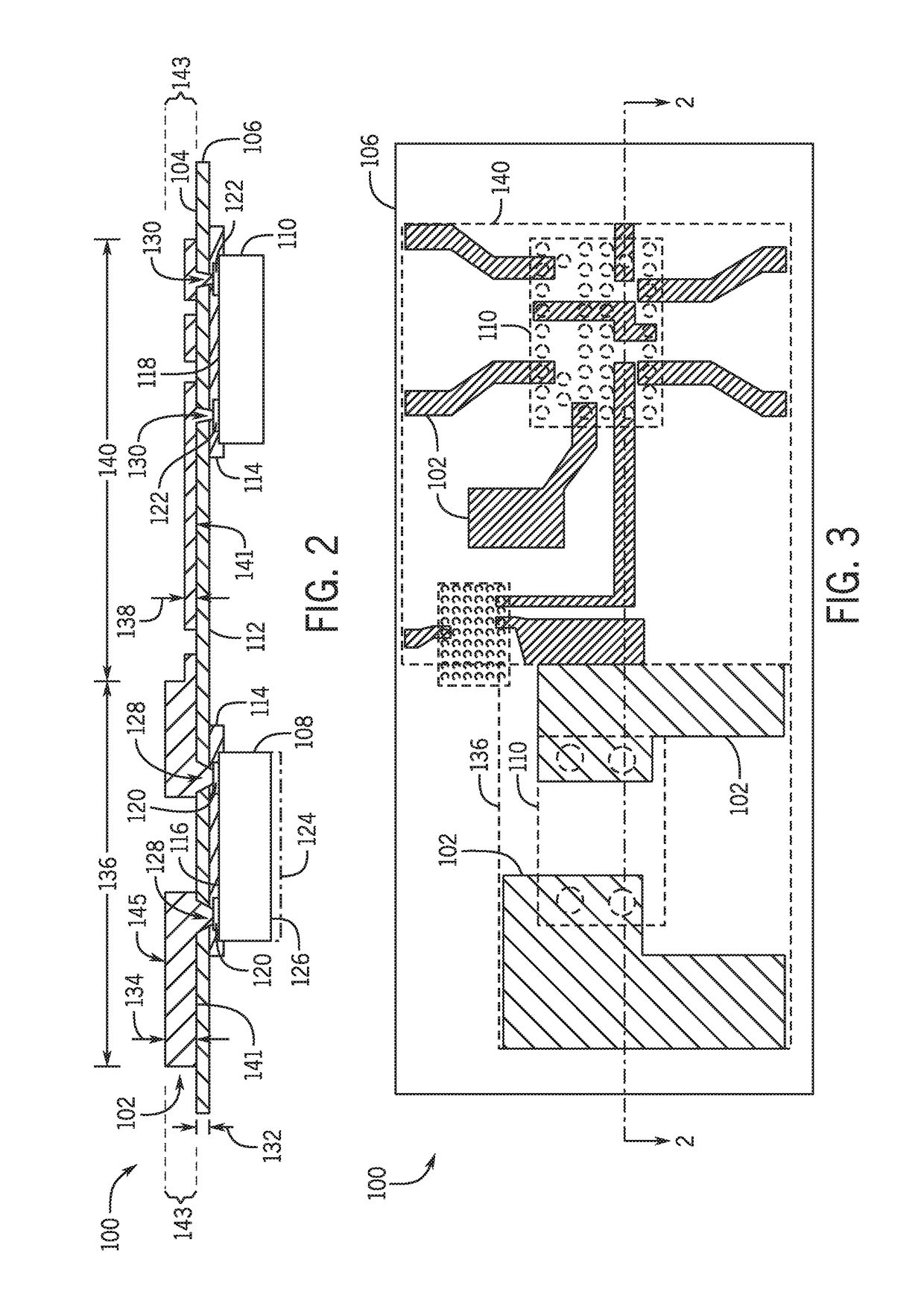
[0030]Embodiments of the present invention provide for an electronics package that includes multiple semiconductor devices, dies, or chips coupled to a patterned conductor layer with locally varied thicknesses. This multi-thickness conductor layer is contained within a common horizontal plane of the electronics package and includes regions having different routing density and current carrying capabilities, the benefits of which may be leveraged for I / O connections to a single electrical component or to multiple electrical components within the electronics package. As described in more detail below, in the case of a multi-chip module portions of the multi-thickness conductor layer include a low density routing pattern that provides the requisite current carrying capabilities for one type of electrical component, such as a power semiconductor die, while other, thinner portions of the conductor layer have a high density routing pattern that enables routing capability below 100 / 100 μm L...
PUM
 Abstract
Description
Claims
Application Information
 - R&D
- Intellectual Property
- Life Sciences
- Materials
- Tech Scout
- Unparalleled Data Quality
- Higher Quality Content
- 60% Fewer Hallucinations
Browse by: Latest US Patents, China's latest patents, Technical Efficacy Thesaurus, Application Domain, Technology Topic, Popular Technical Reports.
© 2025 PatSnap. All rights reserved.Legal|Privacy policy|Modern Slavery Act Transparency Statement|Sitemap|About US| Contact US: help@patsnap.com