Unlock instant, AI-driven research and patent intelligence for your innovation.

Voltage reference buffer circuit

a voltage reference buffer and circuit technology, applied in the field of buffer circuits, can solve the problems of weak driving capability, affecting the signal-to-noise ratio (snr), affecting the size of the circuit area of the voltage reference buffer itself, etc., and achieve the effect of enhancing driving capability

Inactive Publication Date: 2018-05-17
REALTEK SEMICON CORP
View PDF1 Cites 3 Cited by
  • Summary
  • Abstract
  • Description
  • Claims
  • Application Information

AI Technical Summary

Benefits of technology

The invention provides a voltage reference buffer circuit with multiple driving components to improve its driving ability.

Problems solved by technology

Furthermore, the design also affects the signal-to-noise ratio (SNR) and the settling speed of a voltage reference reception circuit, and affects the power consumption and the size of circuit area of the voltage reference buffer itself.
For such voltage reference buffer, the driving capability, especially the capability of current sink, is weak.
However, generally, when the input voltage or a load of the LDO changes rapidly, under the restriction of a limited loop bandwidth of the aforementioned negative feedback mechanism, the aforementioned output transistor cannot respond to the rapid change immediately, then a transient response of the output voltage of the LDO is raised, and thus the output voltage changes suddenly.
This transient change of the output voltage may damage the system; for instance, when the output voltage goes too high, it may damage the components in a following stage of the system, and when the output voltage goes too low, it may affect the normal operation of the following stage.
In light of the above, although some LDO uses two transistors of the same type at a voltage output terminal, one of the transistors (e.g., the aforementioned transistor MPD or the discharge transistor 10) is only turned on when an overvoltage occurs; therefore this transistor is not able to source current to a load terminal or sink current from the load terminal during a normal operation.
As a result, this kind of LDO is by no means to improve its driving capability through additional transistors.

Method used


Image

  • Voltage reference buffer circuit
  • Voltage reference buffer circuit
  • Voltage reference buffer circuit

Examples


Embodiment Construction

[0020]The following description is written by referring to terms acknowledged in this industrial filed. If any term is defined in the description, such term should be explained accordingly. Besides, the connection between objects in the disclosed embodiments of this specification can be direct or indirect provided that these embodiments are still practicable under such connection. Said “indirect” indicates that an intermediate object or a physical space is existed between the objects. In addition, the shape, size, and ratio of any element in the disclosed drawings are just exemplary for understanding rather than restrictive for the present invention.

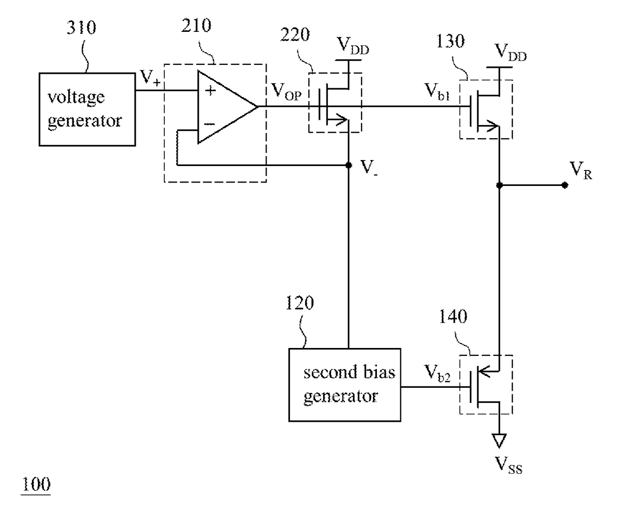
[0021]The present invention discloses a voltage reference buffer circuit using a plurality of driving components for enhancing the capability of souring and sinking current, and achieving the efficacy of prompt operation and low power consumption.

[0022]Please refer to FIG. 1 showing an embodiment of the voltage reference buffer circuit o...


PUM


Abstract

The present invention discloses a voltage reference buffer circuit. An embodiment of the voltage reference buffer circuit includes: a first bias generator configured to generate a first bias voltage; a second bias generator configured to generate a second bias voltage different from the first bias voltage; a first driving component coupled to a high voltage terminal, the first bias generator and a reference voltage output terminal, and configured to control a reference voltage at the reference voltage output terminal according to the first bias voltage; and a second driving component coupled to the reference voltage output terminal, the second bias generator and a low voltage terminal, and configured to control a current between the reference voltage output terminal and the second driving component according to the second bias voltage.

Description

BACKGROUND OF THE INVENTION1. Field of the Invention[0001]The present invention relates to a buffer circuit, especially to a voltage reference buffer circuit.2. Description of Related Art[0002]The design of a voltage reference buffer affects the precision of a reference voltage and the time for establishing the reference voltage. Furthermore, the design also affects the signal-to-noise ratio (SNR) and the settling speed of a voltage reference reception circuit, and affects the power consumption and the size of circuit area of the voltage reference buffer itself.[0003]Generally, at the reference voltage output terminal of a general voltage reference buffer is set a single driving component. For such voltage reference buffer, the driving capability, especially the capability of current sink, is weak. An example of this kind of voltage reference buffer is found in the following literature: Wei-Hsin Tseng, Wei-Liang Lee, Chang-Yang Huang, and Pao-Cheng Chiu, “A 12-bit 104 MS / s SAR ADC i...

Claims


Application Information

Patent Timeline
IPC IPC(8): G05F1/618G05F3/24G05F1/40G05F1/571G05F1/573G05F1/575
CPCG05F1/618G05F3/247G05F1/40G05F1/571G05F1/573G05F1/575
Inventor CHANG, CHE-WEILIU, KAI-YINLEI, LIANG-HUANHUANG, SHIH-HSIUNG
Owner REALTEK SEMICON CORP
Features
  • R&D
  • Intellectual Property
  • Life Sciences
  • Materials
  • Tech Scout
  • Unparalleled Data Quality
  • Higher Quality Content
  • 60% Fewer Hallucinations
Learn More