Display panel

Active Publication Date: 2022-04-07
SHENZHEN CHINA STAR OPTOELECTRONICS SEMICON DISPLAY TECH CO LTD
View PDF0 Cites 0 Cited by
  • Summary
  • Abstract
  • Description
  • Claims
  • Application Information

AI Technical Summary

Benefits of technology

[0031]The beneficial effects of this application are:
[0032]In the display panel provided by the present application, two gate driver on array (GOA) circuit units are arranged side by side between adjacent two rows of pixel units, and the two GOA circuit units arranged side by side are electrically connected to the same row of the pixel units, and bidirectional driving is used to improve the drive capability o

Problems solved by technology

However, as resolutions become higher and pixel sizes become smaller, space for GOA layout becomes larger, and designing the GOA in the AA leads to

Method used


Image

  • Display panel
  • Display panel
  • Display panel

Examples


embodiment 1

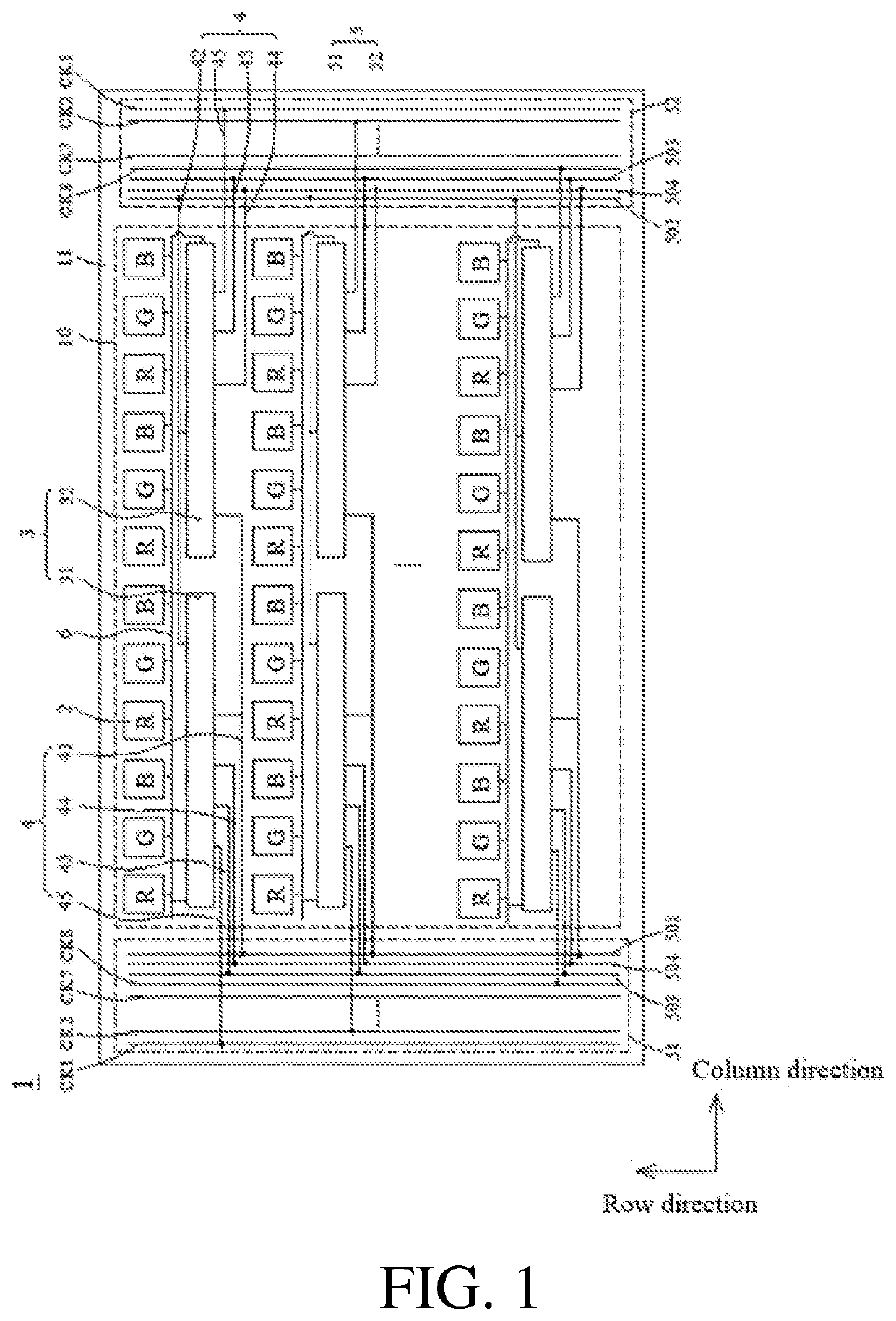
[0049]Please refer to FIG. 1, which is a schematic structural diagram of a display panel according to embodiment 1 of the present application. The display panel 1 includes pixel units 2 arranged in an array in a display area 10, and a GOA circuit unit 3 and signal-connecting lines 4 between two adjacent rows of the pixel units 2. Each stage of the GOA circuit unit 3 is electrically connected to a row of the pixel units 2 through a scan line 6, and the GOA circuit unit 3 is used to provide a gate signal to the pixel unit 2 connected thereto.

[0050]Specifically, two GOA circuit units are arranged side by side in the row direction between the pixel units 2 in two adjacent rows, and the two GOA circuit units arranged side by side are electrically connected to the pixel units 2 in the same row, wherein the two GOA circuit units arranged side by side are respectively the same-stage GOA circuit unit in the two sets of GOA circuits, so the pixel units 2 in the same row can be driven at the s...

embodiment 2

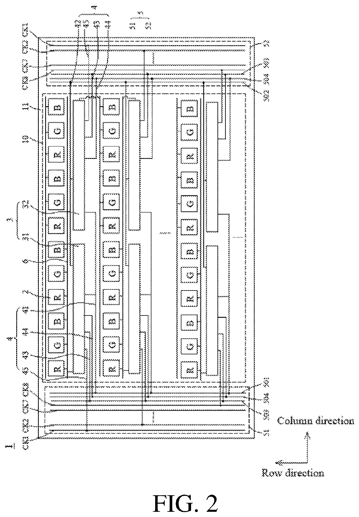
[0064]Please refer to FIG. 2, which is a schematic structural diagram of a display panel according to embodiment 2 of the present application. The structure of the display panel in this embodiment is the same as / similar to the structure of the display panel in the first embodiment above. The only difference is that two GOA circuit units 3 arranged side by side in the display panel of this embodiment are electrically connected to the pixel units 2 in two adjacent rows.

[0065]Specifically, the first GOA circuit unit 31 and the second GOA circuit unit 32 arranged side by side in the row direction differ by one stage in the number of stages. For example, if the first GOA circuit unit 31 is an N stage GOA circuit unit in the first set of GOA circuits, the second GOA circuit unit 32 is an N+1 stage GOA circuit unit in the second set of GOA circuits, wherein N is a positive integer greater than 0. Therefore, the first GOA circuit unit 31 and the second GOA circuit unit 32 arranged side by s...

embodiment 3

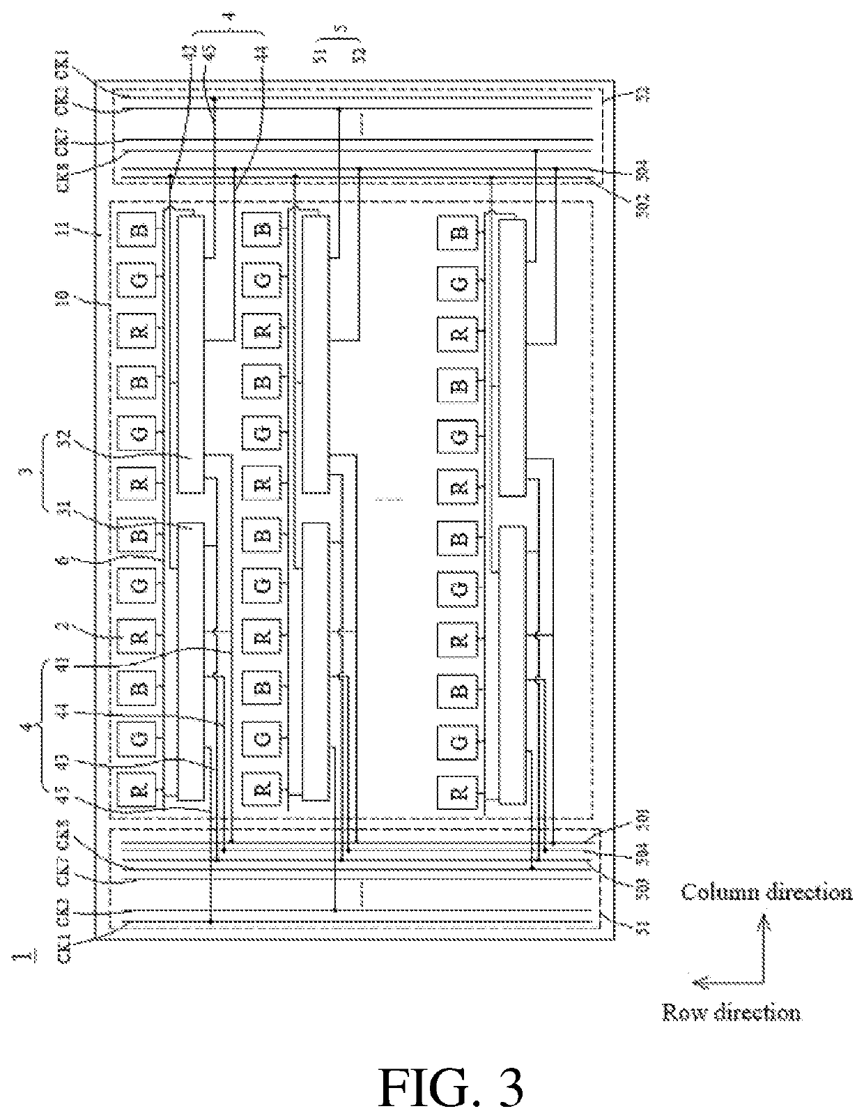
[0069]Please refer to FIG. 3, which is a schematic structural diagram of a display panel provided in embodiment 3 of the present application. The structure of the display panel in this embodiment is the same as / similar to the structure of the display panel in embodiment 1 described above. The only difference is that: two GOA circuit units 3 arranged side by side in the display panel of this embodiment share the reset signal-connecting line 43. In addition, one of the first GOA bus unit 51 and the second GOA bus unit 52 includes a reset signal bus 503, and the other does not include the reset signal bus 503.

[0070]That is, in this embodiment, the reset signal bus 503 transmits a reset signal (RST) to the first GOA circuit unit 31 and the second GOA circuit unit 32 through a common reset signal-connecting line 43, respectively. The first low-frequency clock signal bus 501 transmits the first low-frequency clock signal (LC1) to the first GOA circuit unit 31 and the second GOA circuit un...


PUM


Abstract

The present application provides a display panel. A display area of the display panel includes pixel units, and non-display areas positioned on opposite sides of the display area are provided with a gate driver on array (GOA) bus unit. Two GOA circuit units are arranged side by side between two adjacent rows of the pixel units, and the two GOA circuit units arranged side by side are electrically connected to the pixel units. The GOA circuit units are electrically connected to the GOA bus unit through signal-connecting lines disposed in the display area, and wherein the two GOA circuit units arranged side by side share at least one of the signal-connecting lines. The present application is beneficial for increasing aperture ratio and transmittance of the pixel units.

Description

FIELD OF INVENTION[0001]The present application relates to the field of display technology, in particular to a display panel.BACKGROUND OF INVENTION[0002]Gate driver on array (GOA) technology is a technology of directly manufacturing gate driver circuits (gate driver ICs) on an array substrate to replace an external silicon chip. At present, large-size, high-resolution display products and display products with extremely narrow borders have become market trends. Requirements of narrow widths of four sides of spliced screens are even more extreme. In addition, in order to seek lowest cost and best appearance, a technology of positioning the GOA in an active area (AA) is increasingly favored.[0003]However, as resolutions become higher and pixel sizes become smaller, space for GOA layout becomes larger, and designing the GOA in the AA leads to a decrease in aperture ratio and seriously insufficient transmittance.[0004]Therefore, the current technology has defects that need to be solved...

Claims


Application Information

Patent Timeline
IPC IPC(8): G09G3/20
CPCG09G3/20G09G2300/0408G09G2310/0283G09G2310/061G09G2310/0267G09G2310/08G09G2300/0426G09G2300/0465G09G3/2003
Inventor ZHU, JING
Owner SHENZHEN CHINA STAR OPTOELECTRONICS SEMICON DISPLAY TECH CO LTD
Why Eureka
Try Eureka