Sputter protective layer for organic electronic devices

a technology of organic electronic devices and protective layers, which is applied in the direction of solid-state devices, semiconductor devices, coatings, etc., can solve the problems of difficult scaling up of evaporation, low throughput, and widespread use of industrial manufacturing processes, so as to improve sub-threshold swing, reduce the voltage of turn on, and reduce the threshold voltage value

Pending Publication Date: 2021-04-22
SMARTKEM
View PDF7 Cites 2 Cited by
  • Summary
  • Abstract
  • Description
  • Claims
  • Application Information

AI Technical Summary

Benefits of technology

[0032]The invention aims to protect the OGI from plasma-induced damage by providing a highly cross-linked OSPL coated directly onto the OGI. This in turn, enables OTFT arrays that retain their pre-sputter / plasma electronic characteristics, such as low threshold voltage values (preferably AVth post plasma <2V @ Vg volts (measured in the linear regime), low turn on voltages (preferably Vto post plasma <3V) low off currents (preferably <10−1%), low change in sub-threshold swing values (preferably ΔSS post plasma <0.5V) and high Ion / off ratios (preferably ≥106). Benefits include OTFTs having lower threshold voltage values, lower turn on voltages, improved sub-threshold swing, higher on currents, low off currents and high on / off ratios, all of which enable improved driving capability. Lower off currents reduces leakage currents (and concomitantly power consumption in the off state). Low Vth is required to reduce the gate voltage needed to maintain an OTFT in the off state. Low Vth combined with a low sub-threshold swing reduces power consumption and improves the switching speed of the device.
[0033]The OSPL of the invention preferably has a higher permittivity than the OGI. For example, the OGI material has a dielectric constant (k)<3.0 @ 1000 Hz, preferably <2.5 @ 1000 Hz. The OSPL preferably has a higher permittivity than the OGI layer, typically >1 unit higher than the OGI. The OSPL has a dielectric constant (k)>3.3 @ 1000 Hz, preferably >3.5 @ 1000 Hz, preferably >4.0 @ 1000 Hz. Such higher permittivity is provided by the polar, multi-functional acrylate components of the OSPL ink (discussed in detail below). This feature can advantageously be used to increase the overall capacitance of the OGI / OSPL layer in the active channel region of the transistor. A higher gate capacitance is desirable to reduce device operating voltages. However, this is best achieved by increasing the permittivity rather than reducing the thickness of the OGI, to prevent dielectric breakdown. The dual layer formed by the low permittivity OGI and higher permittivity OSPL has an effective permittivity higher than the OGI, increasing capacitance and maintaining dielectric integrity, whilst retaining the benefit of having a low permittivity insulator directly in contact with the OSC as explained above. The sputter protective layer remains in place in the OSC / OGI channel region of the OTFT throughout the lifetime of the device and is not removed.

Problems solved by technology

However, evaporation is difficult to scale up as uniformity over large areas is poor, throughput is low, and it is therefore not widely used in industrial manufacturing processes.
It is particularly problematic when amorphous polymeric organic materials are being used as the layer directly exposed to plasma.
This is due to bombardment from ions, electrons and UV photons generated during plasma sputtering which cause structural damage to the organic material.
Furthermore, plasma-induced damage to amorphous perfluoropolymer layers was reported in the Journal of Photopolymer Sci & Technology; Vol 27, No. 3, 2014, pp 393-398[1] where it stated that C—F bonds are particularly prone to plasma damage.
These damaged bonds may cross-link or recombine forming defects / dipoles and traps at, or close to the OSC / OGI interface.
When top gate OTFTs comprising materials such as Cytop™ as gate insulator are exposed to plasma sputtering processes, UV photons cause irreversible damage to the chemistry of the Cytop™ layer.
In the OTFT, this damage is manifest as a number of undesirable electrical characteristics including high threshold voltage values (Vth), high turn on voltages (Vto), high subthreshold swing (SS), high off currents, low Ion / off ratios and poor bias stress stability.
The resulting higher operating voltages in turn results in devices having higher power consumption.
Cytop™ is known to suffer damage in an argon plasma.
However, in direct contradiction to the teaching of WO2008 / 131836, we have found that Cytop™ is irreversibly damaged on exposure to even low levels of low energy Ar plasma.
In the case of OTFTs, plasma or chemical treatment would irreversibly damage the OGI and render the OTFT useless.

Method used


Image

  • Sputter protective layer for organic electronic devices
  • Sputter protective layer for organic electronic devices
  • Sputter protective layer for organic electronic devices

Examples


Embodiment Construction

e organic gate insulator (OGI) layer comprises a low permittivity polymer having a dielectric constant (k)3.3, more preferably >3.5, more preferably >4.0 @1000 Hz.

[0048]Preferably, the OSPL has a permittivity (k)>3.3 @ 1000 Hz, preferably k>3.5 and more preferably >4.0 at 1000 Hz. Where more than one OSPL is present, they may have different permittivity to one another. This may be affected by virtue of their relative chemical composition.

[0049]Some examples of low permittivity polymers preferably include perfluoropolymers, benzocyclobutene polymers (BCB), parylene, polyvinylidene fluoride (PVDF) polymers, cyclic olefin copolymers (e.g. norbornene, TOPAS™) polymers, adamantyl polymers, perfluorocyclobutylidene polymers (PFCB), polymethylsiloxane (PDMS), and mixtures thereof.

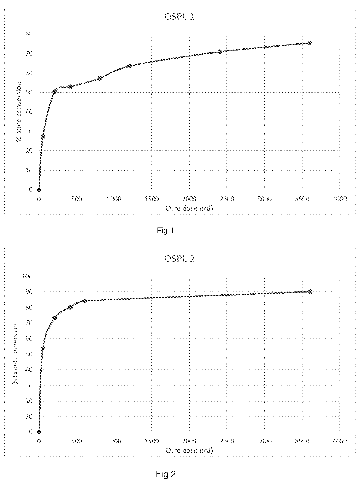
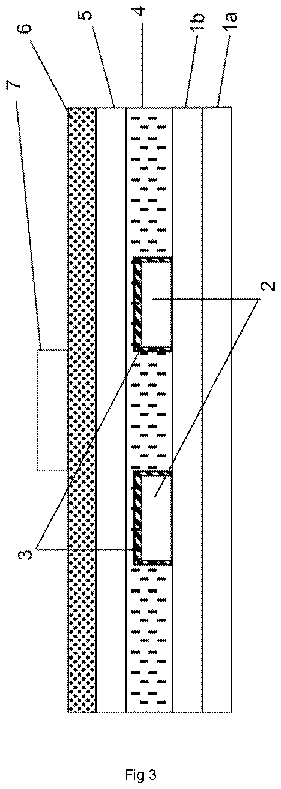
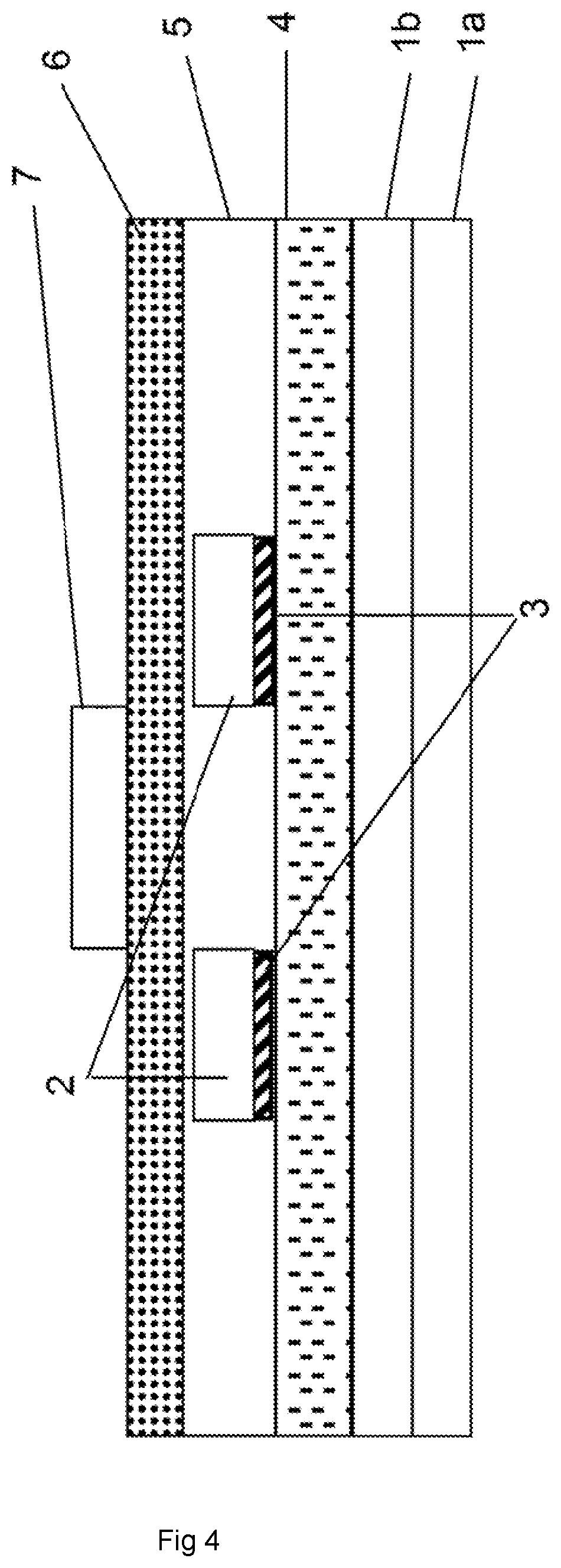
[0050]The crosslinkable OSPL is coated on top of the OGI using any solution coating technique, preferably including spin coating, spray coating, slot-die coating, ink jet printing. The OSPL is crosslinked to provi...


PUM

PropertyMeasurementUnit
thickaaaaaaaaaa
surface free energyaaaaaaaaaa

Abstract

The present invention provides an organic gate insulator (OGI) layer having a low dielectric constant (k), said organic gate insulator layer being over-coated with a cross-linked organic layer (OSPL) having a relatively high permittivity (k). The present invention also provides an electronic device comprising such an organic thin film transistor. The invention also provides a solution for producing said OSPL, and a process for producing said OSPL.

Description

FIELD OF THE INVENTION[0001]The invention relates to electronic devices including organic thin film transistors (OTFTs) comprising a solution-coatable, cross-linkable Organic Sputter Protective Layer (OSPL) in direct contact with a low permittivity organic gate insulator (OGI), wherein the OSPL is incorporated to prevent sputter damage to the OGI during processing of transistors, and provides transistors retaining their pre-plasma electrical performance metrics.BACKGROUND OF THE INVENTION[0002]Thermal evaporation of metals is a commonly used laboratory technique for the deposition of contact electrodes in test arrays of electronic devices. Generally, the source materials are resistively heated to the point where they sublime and condense on to the substrate forming a thin film. There is minimal heat transfer or physical damage to the substrate and the resultant films are usually of high purity due to the lack of any gas inclusion (as in sputtering) and the high vacuum needed for thi...

Claims


Application Information

Patent Timeline
Patent Type & Authority Applications(United States)
IPC IPC(8): H01L51/05H01L51/00C09D4/00C08F230/08C09D143/04
CPCH01L51/052H01L51/0094C09D4/00H01L51/004C09D143/04H01L51/0541H01L51/0043C08F230/08H10K10/471H10K10/474H10K85/40H10K10/464H10K85/141H10K85/151
Inventor LOWMAN, IANMORGAN, JOHNMOHIALDIN-KHAFFAF, SOADWATSON, COLINBROWN, BEVERLEY
Owner SMARTKEM
Why Eureka
Try Eureka