
Volatile semiconductor memory management device

Active Publication Date: 2018-05-24
RISO KAGAKU CORP
View PDF5 Cites 0 Cited by
  • Summary
  • Abstract
  • Description
  • Claims
  • Application Information

AI Technical Summary

Benefits of technology

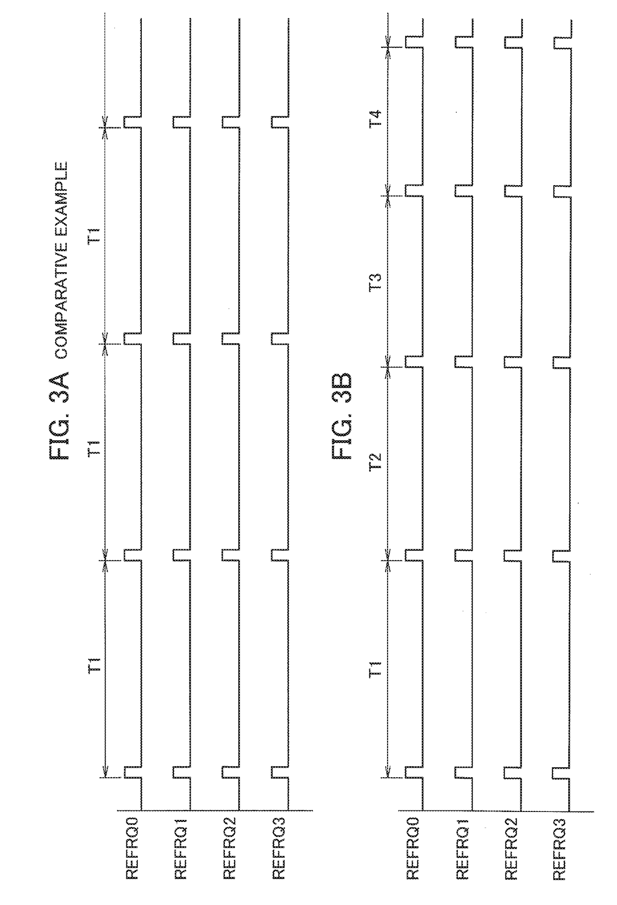
The patent is about a semiconductor memory management device that can minimize the generation of radiation noise during a refresh operation of the DRAM. This device can suppress the power consumption and radiation noise by shifting the timings of the refresh operations of the target cells and reducing the intensity of the radiation noise generated by the change in the current flowing through the DRAM. In simple terms, this device can hold the storage content of the volatile semiconductor memory without causing any damage due to radiation noise.

Problems solved by technology

Power consumption in each cell increases in the refresh operation of the DRAM.

Method used


Image

  • Volatile semiconductor memory management device
  • Volatile semiconductor memory management device
  • Volatile semiconductor memory management device

Examples


Embodiment Construction

[0026]In the following detailed description, for purposes of explanation, numerous specific details are set forth in order to provide a thorough understanding of the disclosed embodiments. It will be apparent, however, that one or more embodiments may be practiced without these specific details. In other instances, well-known structures and devices are schematically shown in order to simplify the drawing.

[0027]Description will be hereinbelow provided for embodiments of the present invention by referring to the drawings. It should be noted that the same or similar parts and components throughout the drawings will be denoted by the same or similar reference signs, and that descriptions for such parts and components will be omitted or simplified. In addition, it should be noted that the drawings are schematic and therefore different from the actual ones.

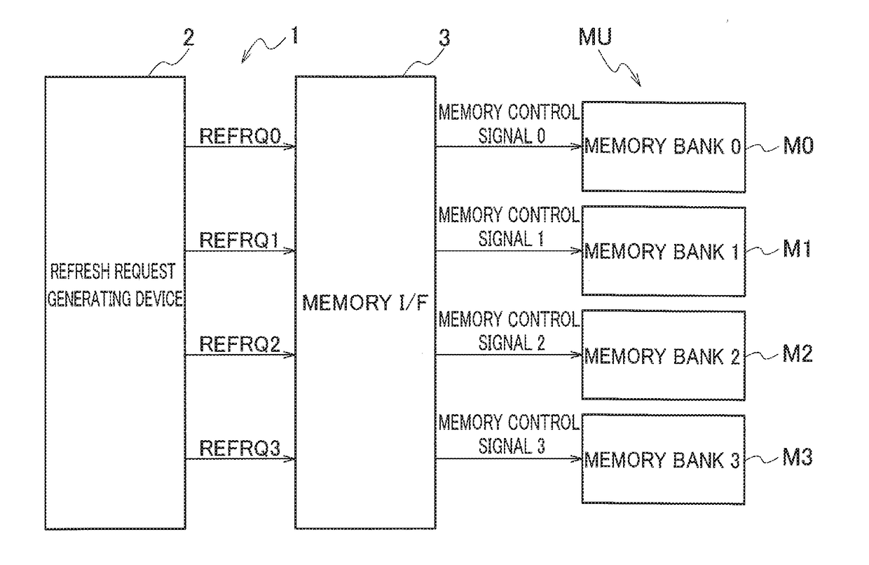
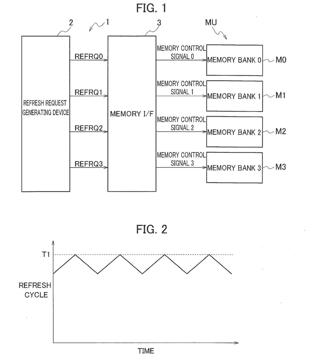
[0028]FIG. 1 is a block diagram illustrating a configuration of a management device 1 of a semiconductor memory according to an embodi...


PUM


Abstract

A management device for a volatile semiconductor memory includes: a request generator configured to output a refresh request requesting a refresh operation of a target cell in the volatile semiconductor memory; and a refresh operator configured to execute the refresh operation of the target cell requested in the refresh request outputted by the request generator. The request generator repeatedly outputs the refresh request for a same target cell in the volatile semiconductor memory intermittently at unequal intervals with each two successive intervals being different from each other.

Description

CROSS REFERENCE TO RELATED APPLICATION[0001]This application is based upon and claims the benefit of priority from the prior Japanese Patent Application No. 2016-226634, filed on Nov. 22, 2016, the entire contents of which are incorporated herein by reference.BACKGROUND1. Technical Field[0002]The disclosure relates to a management device of a volatile semiconductor memory for which a refresh operation is required to keep holding a stored content.2. Related Art[0003]As a volatile semiconductor memory, there is a semiconductor memory which dynamically stores data (DRAM). The DRAM has multiple cells each formed by combining a transistor and a capacitor. Each cell stores and holds data by using a charge accumulated in the capacitor.[0004]Accordingly, in order to keep storing data in the DRAM, the DRAM has to repeatedly perform a refresh operation of storing the data again by accumulating a charge in the capacitor at certain intervals, before the charge accumulated in the capacitor leaks...

Claims


Application Information

Patent Timeline
IPC IPC(8): G11C11/406G06F3/06
CPCG11C11/40611G06F3/0604G06F3/0659G06F3/0673G11C11/40618
Inventor YOSHINO, YUJI
Owner RISO KAGAKU CORP
Learn More