Image sensor and control method of image sensor, and image capturing apparatus

Pending Publication Date: 2020-10-22
CANON KK
View PDF3 Cites 1 Cited by
  • Summary
  • Abstract
  • Description
  • Claims
  • Application Information

AI Technical Summary

Benefits of technology

[0007]The present invention has been made in consideration of the above situation, and suppresses aver

Problems solved by technology

In such an APD, when a single photon is incident while a reverse bias voltage larger than a breakdown voltage is applied, carriers generated by the incident photon cause avalanche multiplication and large current is generated.
A problem that when photons continue to be incident on an image sensor, in particular, having a large number of pixels, such current is repeatedly generated in many pixels, and power consumption greatly increas

Method used


Image

  • Image sensor and control method of image sensor, and image capturing apparatus
  • Image sensor and control method of image sensor, and image capturing apparatus
  • Image sensor and control method of image sensor, and image capturing apparatus

Examples


Example

First Embodiment

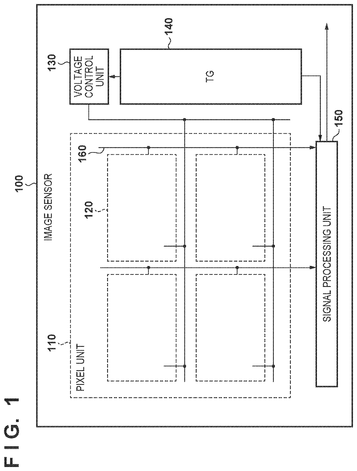
[0024]Hereinafter, a configuration of an image sensor 100 according to the first embodiment and a control method thereof will be described with reference to FIG. 1.

[0025]In FIG. 1, the image sensor 100 includes a pixel unit 110, pixels 120, a voltage control unit 130, a timing control unit (hereinafter, referred to as “TG”) 140, and a signal processing unit 150.

[0026]In the pixel unit 110, a plurality of pixels 120 are arranged, and data transfer lines 160 are provided for respective columns. Each pixel 120 includes a SPAD (Single Photon Avalanche Diode) and counts photons incident on the SPAD. The count value, which is the counted data, is transferred to the signal processing unit 150 via the data transfer line 160. Although four pixels 120 are shown in FIG. 1 for the sake of explanation, a very large number of pixels 120 are actually arranged in a matrix to form the pixel unit 110.

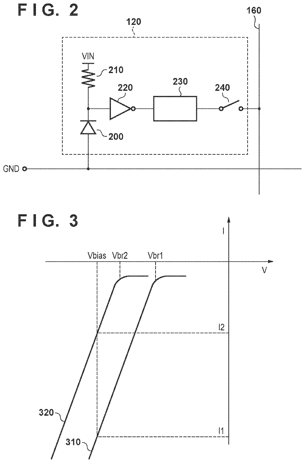
[0027]The voltage control unit 130 controls the reverse bias voltage Vbias applied to...

Example

Second Embodiment

[0056]Next, a method for controlling the image sensor 100 according to the second embodiment of the present invention will be described with reference to FIG. 7. Note that the configuration of the image sensor 100 in the second embodiment is the same as that described in the first embodiment, and a description thereof will be omitted. In the following description, points that are different from the first embodiment will be described.

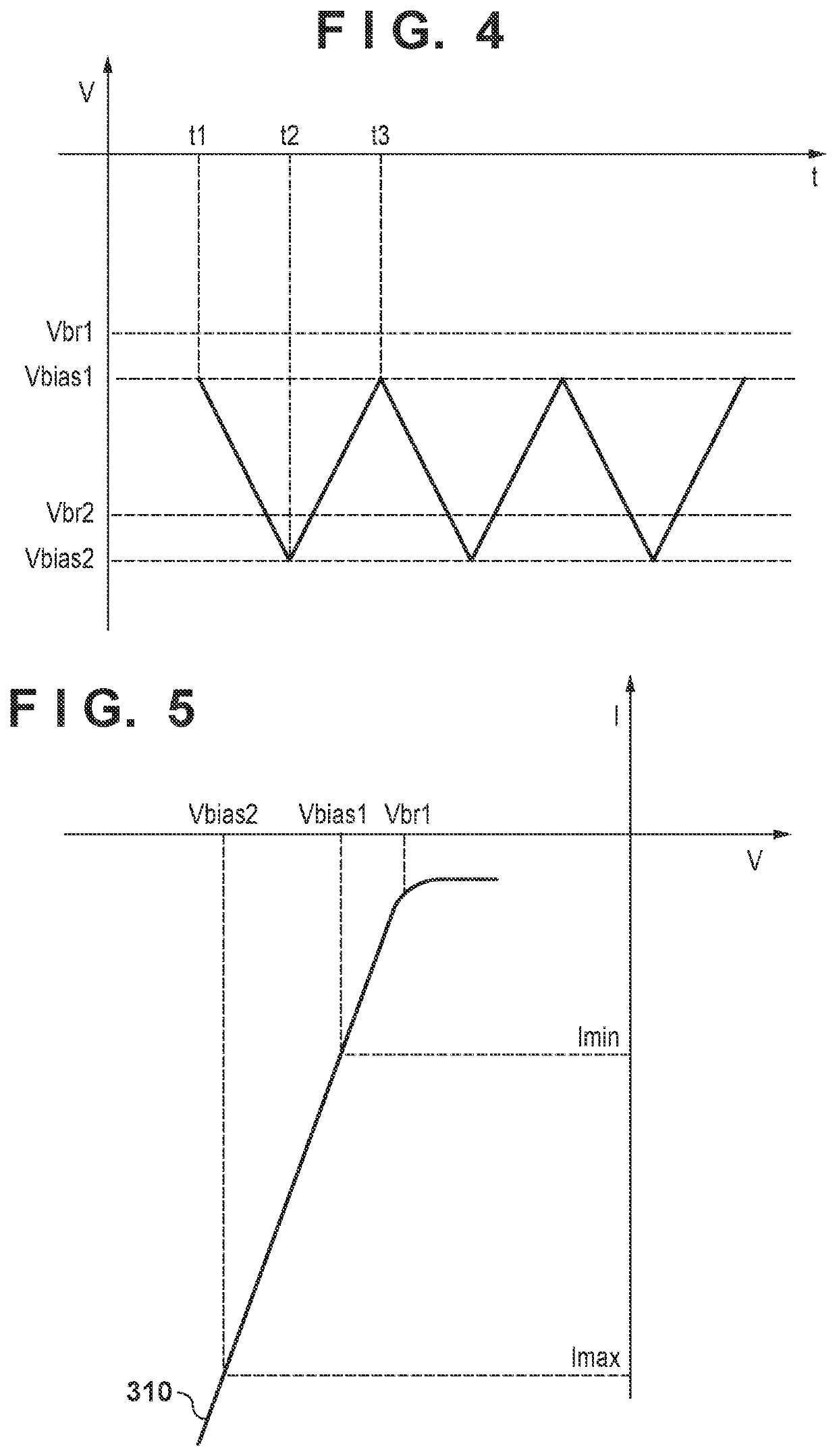
[0057]FIG. 7 is a diagram illustrating the reverse bias voltage Vbias controlled by the voltage control unit 130 in a state for detecting photons, as in FIG. 4. The reverse bias voltage Vbias periodically changes between the minimum reverse bias voltage Vbias1 and the maximum reverse bias voltage. Here, a case where a periodically changing reverse bias voltage is applied to the SPAD 200b having a large breakdown voltage will be described.

[0058]First, at time t11, the voltage control unit 130 controls the reverse bias voltage Vbias applie...

Example

Third Embodiment

[0071]Next, a third embodiment of the present invention will be described. FIG. 8 is a block diagram illustrating a schematic configuration of an image capturing apparatus. The image sensor 100 described in the first and second embodiments is used as an image sensor 1101.

[0072]A lens driving circuit 1109 performs zoom control, focus control, and diaphragm control for an imaging lens unit 1110, and the imaging lens unit 1110 forms an optical image of a subject on the image sensor 1101. The image of the subject formed on the image sensor 1101 is converted into an electrical image signal, and then the image signal is output from the image sensor 1101. A signal processing circuit 1103 performs various types of corrections on the image signal output from the image sensor 1101, and compresses data.

[0073]A timing generator 1102 outputs a timing signal that drives the image sensor 1101. An overall control / arithmetic circuit 1104 performs various types of arithmetic operation...


PUM


Abstract

An image sensor comprises: a plurality of pixels each having an avalanche photodiode; and a control unit that controls to provide to the avalanche photodiodes of the plurality of pixels a reverse bias voltage that periodically changes.

Description

BACKGROUND OF THE INVENTIONField of the Invention[0001]The present invention relates to an image sensor which uses an avalanche photodiode, a control method of an image sensor, and an image capturing apparatus.Description of the Related Art[0002]Conventionally, there is a light receiving element that operates an avalanche photodiode (APD) in a Geiger mode to detect a single photon. In such an APD, when a single photon is incident while a reverse bias voltage larger than a breakdown voltage is applied, carriers generated by the incident photon cause avalanche multiplication and large current is generated. Based on this current, it is possible to detect that a single photon is incident on the APD. Such an APD is called a SPAD (Single Photon Avalanche Diode).[0003]In an image sensor using a SPAD in a pixel, large current is generated each time a photon is incident as described above. A problem that when photons continue to be incident on an image sensor, in particular, having a large n...

Claims


Application Information

Patent Timeline
IPC IPC(8): H01L27/146
CPCH01L27/14645H01L27/14609H04N25/76H04N25/709H04N25/773H04N25/779
Inventor OHSHITANAI, KAZUKI
Owner CANON KK
Why Eureka
Try Eureka