Integrated inductor and method for manufacturing the same

Inactive Publication Date: 2018-05-31
REALTEK SEMICON CORP
View PDF20 Cites 0 Cited by
  • Summary
  • Abstract
  • Description
  • Claims
  • Application Information

AI Technical Summary

Benefits of technology

The present disclosure provides a solution to the problems of 8-shaped inductors occupying too much area in a chip, and having a lower quality factor. The integrated inductor is placed in a trench of the substrate, which blocks EMI radiation and improves the quality factor of the inductor. Additionally, patterned ground shields (PGS) can be added to enhance insulation ability for coupling other wires. This results in an improved performance of the integrated inductor and reduced size of electronic products.

Problems solved by technology

However, with miniaturization of electronic products, the 8-shaped inductors still occupy some area in the chip, which is harmful to miniaturization of electronic products.
In view of the foregoing, problems and disadvantages are associated with existing products that require further improvement.
However, those skilled in the art have yet to find a solution.

Method used


Image

  • Integrated inductor and method for manufacturing the same
  • Integrated inductor and method for manufacturing the same
  • Integrated inductor and method for manufacturing the same

Examples


Embodiment Construction

[0020]The detailed description provided below in connection with the appended drawings is intended as a description of the present examples and is not intended to represent the only forms in which the present example may be constructed or utilized. The description sets forth the functions of the example and the sequence of steps for constructing and operating the example. However, the same or equivalent functions and sequences may be accomplished by different examples.

[0021]Unless otherwise defined herein, scientific and technical terminologies employed in the present disclosure shall have the meanings that are commonly understood and used by one of ordinary skill in the art. Unless otherwise required by context, it will be understood that singular terms shall include plural forms of the same and plural terms shall include singular forms of the same.

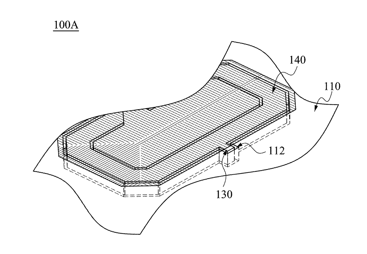
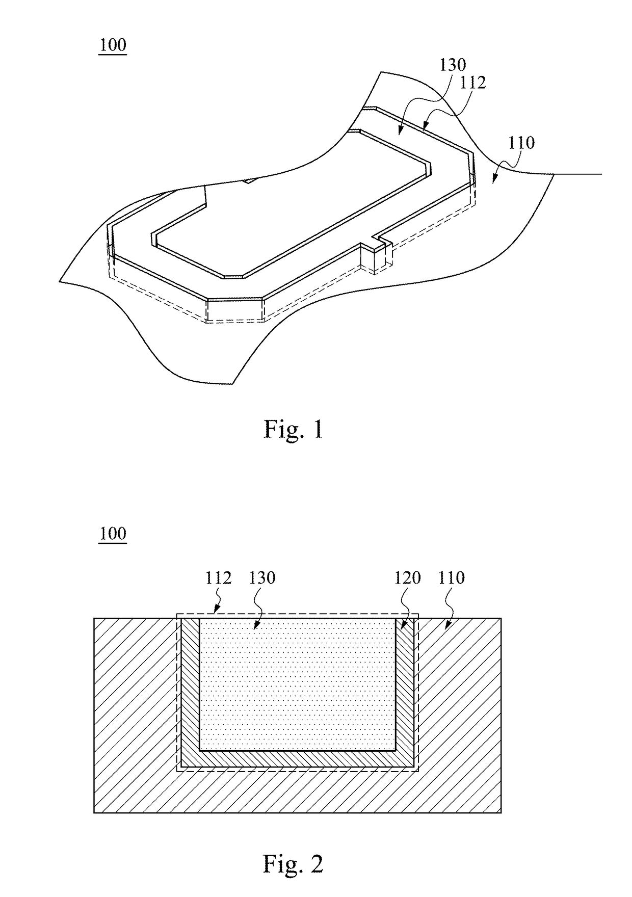
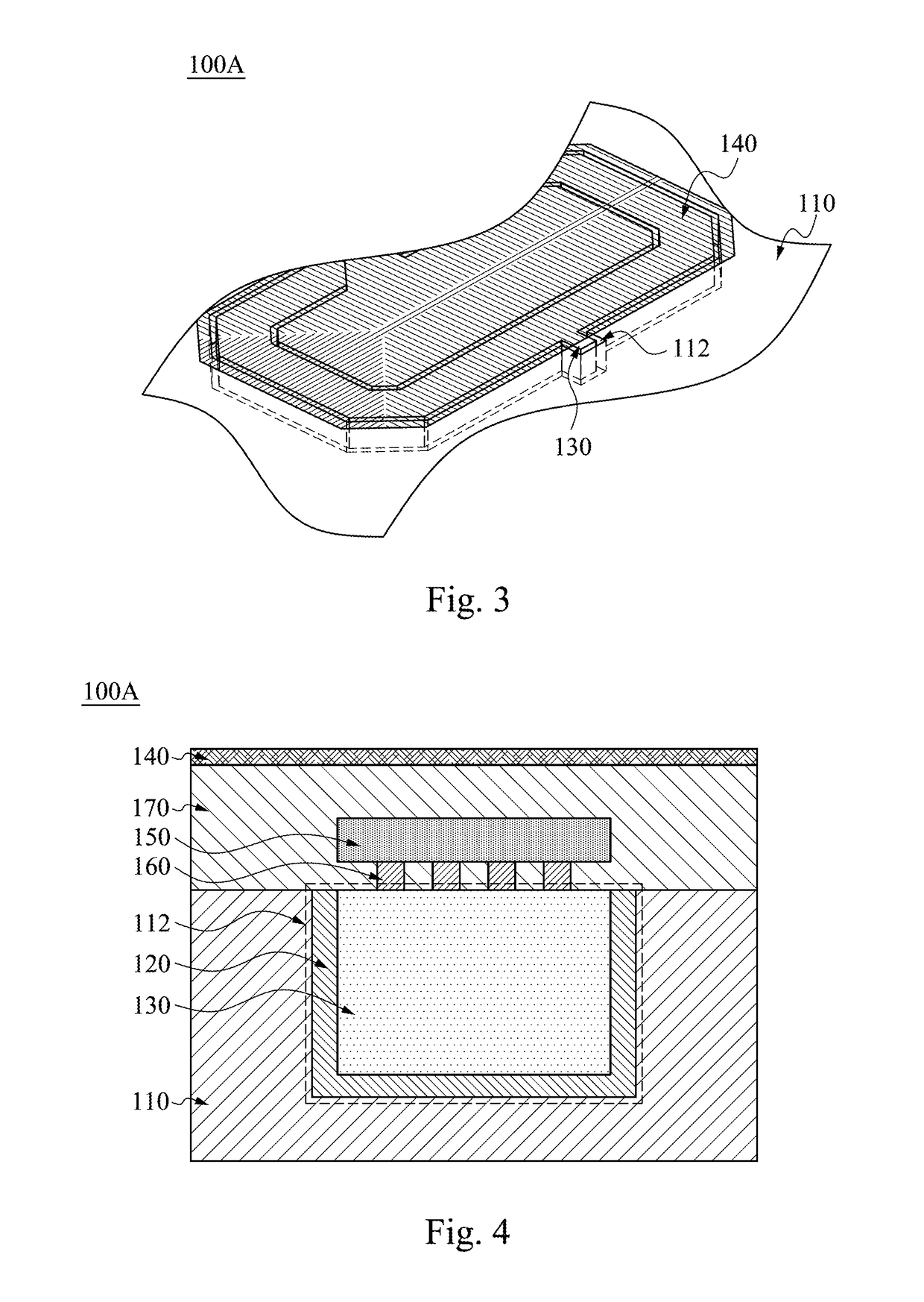
[0022]FIG. 1 is a schematic diagram of an inductor structure 100 according to embodiments of the present disclosure. FIG. 2 is a sectio...


PUM


Abstract

An integrated inductor is disclosed herein. The integrated inductor includes a substrate, an insulation layer, and an inductor. The substrate includes a trench. At least a portion of the insulation layer is formed in the trench. The inductor is disposed in the trench, and the inductor is disposed on the insulation layer.

Description

RELATED APPLICATIONS[0001]This application claims priority to Taiwan Application Serial Number 105138910, filed Nov. 25, 2016, which is herein incorporated by reference.BACKGROUNDField of Invention[0002]The present disclosure relates to a basic electronic circuit. More particularly, the present disclosure relates to an inductor structure and a method for manufacturing the same.Description of Related Art[0003]Conventional inductors occupy large area in a chip, and are easy to have EMI radiation issue. Therefore, 8-shaped inductors arise at an opportune time due to its low EMI radiation possibility and its structure property for neutralizing coupling, such that 8-shaped inductors usually have low mutual coupling value.[0004]However, with miniaturization of electronic products, the 8-shaped inductors still occupy some area in the chip, which is harmful to miniaturization of electronic products. In addition, compared to the conventional inductors, the quality factor of the 8-shaped indu...

Claims


Application Information

Patent Timeline
IPC IPC(8): H01F27/36H01F27/28H01F27/29H01F27/32H01F41/04H01F41/12
CPCH01F27/36H01F27/2804H01F27/29H01F27/32H01F41/041H01F41/12H01F17/0006H01F2017/008
Inventor YEN, HSIAO-TSUNGJEAN, YUH-SHENGYEH, TA-HSUN
Owner REALTEK SEMICON CORP
Why Eureka
Try Eureka