
Light emitting device package structure and manufacturing method thereof

a technology of light emitting devices and package structures, which is applied in the direction of semiconductor/solid-state device manufacturing, semiconductor devices, electrical devices, etc., can solve the problems of inability to the packaging structure may not be reduced efficiently, and the led package structure cannot meet modern needs of miniaturization, so as to achieve the effect of increasing the forward light emitting efficiency of the light emitting device and reducing the thickness and manufacturing cost of the packag

Inactive Publication Date: 2018-05-31
GENESIS PHOTONICS
View PDF6 Cites 0 Cited by
  • Summary
  • Abstract
  • Description
  • Claims
  • Application Information

AI Technical Summary

Benefits of technology

[0004]The invention provides a light emitting device package structure, which does not require a conventional carrying support to be adopted, and may have a thinner package thickness and meet miniaturization requirements.
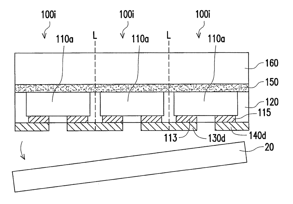
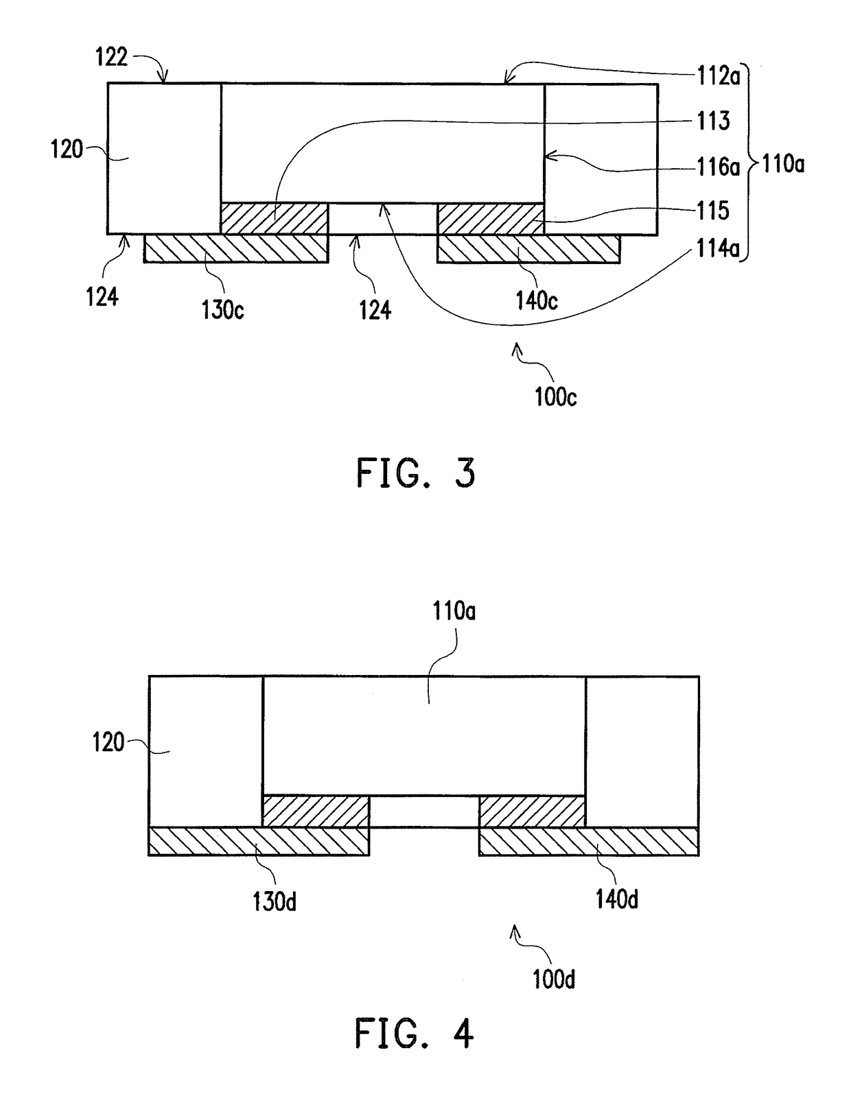
[0009]Based on the above, because the protecting element of the invention encapsulates the side surface of the light emitting device, and the bottom surface of the protecting element is aligned with the first bottom surface of the first electrode pad and the second bottom surface of the second electrode pad of the light emitting device, therefore the light emitting device package structure of the invention does not require a conventional carrying support to support and fix the light emitting device, and may effectively lower the thickness and manufacturing cost of the package. At the same time, the forward light emitting efficiency of the light emitting device can also be effectively increased.

Problems solved by technology

However, the carrying base of the concave cup shape has a particular thickness, such that a thickness of the LED package structure may not be reduced efficiently, therefore causing the LED package structure to be unable to meet modern needs of miniaturization.

Method used


Image

  • Light emitting device package structure and manufacturing method thereof
  • Light emitting device package structure and manufacturing method thereof
  • Light emitting device package structure and manufacturing method thereof

Examples


Embodiment Construction

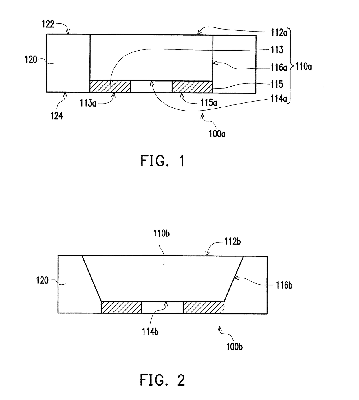
[0024]FIG. 1 is a schematic diagram illustrating a light emitting device package structure according to an embodiment of the invention. Referring to FIG. 1, in the present embodiment, a light emitting device package structure 100a includes a light emitting device 110a and a protecting element 120. The light emitting device 110a has an upper surface 112a and a lower surface 114a opposite to each other, a side surface 116a connecting the upper surface 112a and the lower surface 114a and a first electrode pad 113 and a second electrode pad 115 located on the lower surface 114a and separated from each other. The protecting element 120 encapsulates the side surface 116a of the light emitting device 110a and exposes at least portion of the upper surface 112a, at least portion of a first bottom surface 113a of the first electrode pad 113 and at least portion of a second bottom surface 115a of the second electrode pad 115.

[0025]More specifically, as shown in FIG. 1, the upper surface 112a o...


PUM


Abstract

A light emitting device package structure and a manufacturing method thereof are provided. The light emitting device package structure includes a light emitting device and a protecting element. The light emitting device has an upper surface and a lower surface opposite to each other, a side surface connecting the upper surface and the lower surface and a first electrode pad and a second electrode pad located on the lower surface and separated from each other. The protecting element encapsulates the side surface of the light emitting device and exposes at least portion of the upper surface, at least portion of a first bottom surface of the first electrode pad and at least portion of a second bottom surface of the second electrode pad.

Description

CROSS-REFERENCE TO RELATED APPLICATION[0001]This application is a continuation application of and claims the priority benefit of U.S. application Ser. No. 14 / 711,798, filed on May 14, 2015, now pending. The prior U.S. application Ser. No. 14 / 711,798 claims the priority benefits of Taiwan application serial no. 103116987, filed on May 14, 2014, and U.S. provisional application Ser. No. 62 / 157,450, filed on May 5, 2015. The entirety of each of the above-mentioned patent applications is hereby incorporated by reference herein and made a part of this specification.BACKGROUND OF THE INVENTION1. Field of the Invention[0002]The invention relates to a light emitting device package structure and a manufacturing method thereof, and relates particularly to a light emitting diode package structure and a manufacturing method thereof.2. Description of Related Art[0003]Generally speaking, in a light emitting diode (LED) package structure typically a light emitting diode (LED) chip is disposed on a...

Claims


Application Information

Patent Timeline
Patent Type & Authority Applications(United States)
IPC IPC(8): H01L33/48H01L33/50H01L33/38H01L33/62H01L33/52H01L33/56
CPCH01L33/502H01L2224/18H01L2933/0016H01L2933/0041H01L33/38H01L2933/005H01L2224/32225H01L2224/04105H01L2924/18162H01L2224/73267H01L2224/9222H01L33/62H01L33/50H01L33/486H01L33/52H01L33/56H01L33/005H01L33/48H01L2933/0066H01L2933/0033H01L2224/19H01L21/568
Inventor LEE, HAO-CHUNGLIN, YU-FENG
Owner GENESIS PHOTONICS
Learn More