Thin film transistor and display device using the same

Active Publication Date: 2018-06-07
JAPAN DISPLAY INC
View PDF1 Cites 0 Cited by
  • Summary
  • Abstract
  • Description
  • Claims
  • Application Information

AI Technical Summary

Benefits of technology

[0009]The purpose of the present invention is to avoid an irregularity in Ids characteristics of the TFT without inducing instability in characteristic

Problems solved by technology

The structure of the patent document 1 is to suppress a current at the edge of the channel of the TFT by making a resistance at the edge of the channel large, thus, to prevent the Ids c

Method used


Image

  • Thin film transistor and display device using the same
  • Thin film transistor and display device using the same
  • Thin film transistor and display device using the same

Examples


Example

First Embodiment

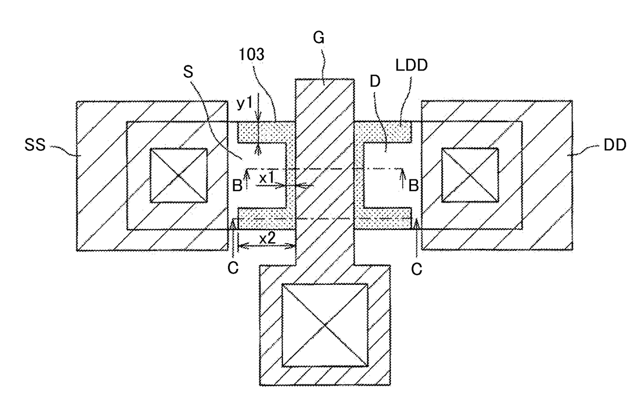
[0040]FIG. 6 is a plan view of the TFT according to the present invention. The structure of the semiconductor layer 103, the gate electrode G, the source area S, the drain area D, the source electrode SS and the drain electrode DD is the same as explained in FIG. 2. The channel is formed under the gate electrode G; the channel has a channel length and a channel width. FIG. 6 differs from FIG. 2 in the structure of the LDD. In FIG. 6, the width x2 of the LDD in the channel length direction at the edge of the semiconductor layer 103 is bigger than the width x1 of the LDD in the channel length direction at the center of the semiconductor layer 103. The structure of FIG. 6 can suppress the influence of an abnormal field at the edge of the semiconductor layer 103 to the channel of the semiconductor layer 103, thus, the abnormal current can be suppressed.

[0041]In FIG. 6, the width x1 of the LDD at the center of the semiconductor layer 103 is e.g. 0.5 μm to 1.5 μm. The widt...


PUM


Abstract

The purpose of the invention is to eliminate an abnormal current at an edge of a semiconductor layer in a thin film transistor. The invention is: A thin film transistor having a semiconductor layer comprising: a channel, a drain and a source are formed in the semiconductor layer, the channel has a channel length and a channel width, a LDD (Light Doped Drain) is formed between the channel and the drain or between the channel and the source, the LDD including a first LDD area, which is formed at a center of the LDD in the direction of the channel width, and a second LDD area, which is formed at an edge of the LDD in the direction of the channel width, wherein a width of the second LDD area in the channel length direction is bigger than a width of the first LDD area in the channel length direction.

Description

CLAIM OF PRIORITY[0001]The present application claims priority from Japanese Patent Application JP 2016-237575 filed on Dec. 7, 2016, the content of which is hereby incorporated by reference into this application.BACKGROUND OF THE INVENTION(1) Field of the Invention[0002]The present invention relates to display devices like a liquid crystal display device or an organic EL display device that use thin film transistors.(2) Description of the Related Art[0003]A liquid crystal display device has a Thin Film Transistor (herein after TFT) in each of the pixels to control taking data in the pixel. Sometimes a driving circuit is formed by TFTs.[0004]An organic EL display device has a first TFT as a switching element to control taking data in the pixel, and a second TFT that controls a current to the light emitting element. Sometimes a driving circuit is formed by TFTs.[0005]Therefore, current-voltage characteristics of the TFTs have a significant influence to characteristics of the liquid c...

Claims


Application Information

Patent Timeline
IPC IPC(8): H01L29/786H01L27/12H01L29/66H01L21/266G09G3/3233G09G3/36
CPCH01L29/78621H01L27/1222H01L27/127H01L29/78696H01L29/78675H01L29/66757H01L21/266H01L27/1288G09G3/3233G09G3/3648H01L27/3262G02F1/1368G02F2001/13685H01L21/26513G02F1/136286H01L27/124H01L27/3276G02F2202/104H01L27/1255H01L2227/323G02F1/13439G02F1/133512G02F1/133514G02F2001/133519G09G2300/0842G09G2320/0233G09G2300/0871G09G2300/0426H10K59/12G02F1/13685G02F1/133519H10K59/131H10K59/1201H10K59/1213
Inventor OKADA, TAKASHI
Owner JAPAN DISPLAY INC
Why Eureka
Try Eureka