Insulated gate switching device and method for manufacturing the same

a technology of insulating gate and switching device, which is applied in the direction of semiconductor device, basic electric element, electrical apparatus, etc., can solve the disadvantage of reducing the effect of suppressing the electric field applied to the gate insulating layer, and achieve the effect of high electric field

Active Publication Date: 2018-06-21
TOYOTA JIDOSHA KK +1
View PDF0 Cites 10 Cited by
  • Summary
  • Abstract
  • Description
  • Claims
  • Application Information

AI Technical Summary

Benefits of technology

[0013]In this insulated gate switching device, the width of the electric field relaxation region is wider than the width of the trench, and hence the electric field relaxation region protrudes in the lateral direction from the gate insulating layer at the lateral surface of the trench. Accordingly, a high electric field is difficult to be applied to the gate insulating layer. Moreover, in this insulated gate switching device, the lower end of the first portion of the body region is located on the lower side with respect to the lower end of the second portion. Accordingly, a region where the second region and the gate insulating layer are in contact with each other is small. The electric field applied to the gate insulating layer can thereby be suppressed more effectively.

Problems solved by technology

If the protruding amount of the electric field relaxation region is small, an effect of suppressing an electric field applied to the gate insulating layer is disadvantageously decreased.

Method used


Image

  • Insulated gate switching device and method for manufacturing the same
  • Insulated gate switching device and method for manufacturing the same
  • Insulated gate switching device and method for manufacturing the same

Examples


embodiment 1

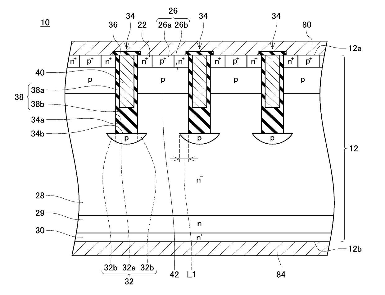
[0040]A MOSFET 10 in Embodiment 1 shown in FIG. 1 has a SiC semiconductor substrate 12. A source electrode 80 is formed on a front surface 12a of the SiC semiconductor substrate 12. A drain electrode 84 is formed on a rear surface 12b of the SiC semiconductor substrate 12.

[0041]A plurality of gate trenches 34 is formed in the front surface 12a of the SiC semiconductor substrate 12. Each of the gate trenches 34 extends long in a direction vertical to a paper surface of FIG. 1. A gate insulating layer 38 and a gate electrode 40 are formed in each gate trench 34. The gate insulating layer 38 includes a bottom insulating layer 38b and a lateral insulating film 38a. The bottom insulating layer 38b is a thick insulating layer formed at a bottom of the gate trench 34. A portion of a lateral surface 34a of the gate trench 34 located on an upper side with respect to the bottom insulating layer 38b is covered with the lateral insulating film 38a. The lateral insulating film 38a is linked to t...

embodiment 2

[0068]In a MOSFET in Embodiment 2 shown in FIG. 11, a density of n-type impurities in a gate adjacent portion 27a of the low-density body region 26b that is in contact with the gate insulating layer 38 is higher than a density of n-type impurities in a gate non-adjacent portion 27b that is apart from the gate insulating layer 38. Notably, the gate non-adjacent portion 27b is adjacent to the gate adjacent portion 27a on an opposite side from the gate insulating layer 38. A lower end of the gate adjacent portion 27a (i.e., a pn junction 42a at a boundary between the gate adjacent portion 27a and the drift region 28) is located on an upper side with respect to a lower end of the gate non-adjacent portion 27b (i.e., a pn junction 42b at a boundary between the gate non-adjacent portion 27b and the drift region 28). Moreover, a density of n-type impurities in a portion 28a of the drift region 28 that is in contact with the gate insulating layer 38 is higher than a density of n-type impuri...

embodiment 3

[0073]In a MOSFET in Embodiment 3 shown in FIG. 17, the density of n-type impurities in the gate adjacent portion 27a of the low-density body region 26b is lower than the density of n-type impurities in the gate non-adjacent portion 27b. The lower end of the gate adjacent portion 27a (i.e., the pn junction 42a at the boundary between the gate adjacent portion 27a and the drift region 28) is located on a lower side with respect to the lower end of the gate non-adjacent portion 27b (i.e., the pn junction 42b at the boundary between the gate non-adjacent portion 27b and the drift region 28). Moreover, the density of n-type impurities in the portion 28a of the drift region 28 that is in contact with the gate insulating layer 38 is lower than the density of n-type impurities in the portion 28b that is apart from the gate insulating layer 38.

[0074]In the MOSFET in Embodiment 3, the lower end of the gate adjacent portion 27a is located on the lower side with respect to the lower end of the...


PUM


Abstract

A method for manufacturing an insulated gate switching device is provided. The method includes: forming a first trench in a surface of a first SiC semiconductor layer; implanting p-type impurities into a bottom surface of the first trench; depositing a second SiC semiconductor layer on an inner surface of the first trench to form a second trench; and forming a gate insulating layer, a gate electrode, a first region and a body region so that the gate insulating layer covers an inner surface of the second trench, the gate electrode is located in the second trench, the first region is of n-type and in contact with the gate insulating layer, the body region is of p-type, separated from the implanted region, and in contact with the gate insulating layer under the first region.

Description

CROSS-REFERENCE TO RELATED APPLICATION[0001]This application claims priority to Japanese Patent Application No. 2015-118389 filed on Jun. 11, 2015, the entire contents of which are hereby incorporated by reference into the present application.TECHNICAL FIELD[0002]A technology disclosed herein relates to an insulated gate switching device and a method for manufacturing the same.BACKGROUND ART[0003]An insulated gate switching device such as a MOSFET (metal oxide semiconductor field effect transistor) or an IGBT (Insulated Gate Bipolar Transistor) has been known. While the insulated gate switching device is turned off, an electric field is applied to a gate insulating film. If the electric field applied to the gate insulating film exceeds an insulation resistance of the gate insulating film, a current flows penetrating the gate insulating film, which is problematic. Accordingly, a technique to relax an electric field applied to the gate insulating film is needed.[0004]Japanese Patent A...

Claims


Application Information

Patent Timeline
Patent Type & Authority Applications(United States)
IPC IPC(8): H01L29/16H01L21/04H01L21/02H01L29/423H01L29/36H01L29/06H01L29/78H01L29/66H01L29/739
CPCH01L29/1608H01L21/0475H01L21/046H01L21/02529H01L29/4236H01L29/36H01L29/0623H01L29/7813H01L29/42368H01L29/66068H01L21/049H01L29/66734H01L29/7397H01L29/66348H01L29/1095
Inventor TAKAYA, HIDEFUMIMIZUNO, SHOJIWATANABE, YUKIHIKOAOI, SACHIKO
Owner TOYOTA JIDOSHA KK
Why Eureka
Try Eureka