Method of manufacturing polymer printed circuit board

a technology of printed circuit board and manufacturing method, which is applied in the direction of printed circuit, printed circuit dielectrics, circuit lamination, etc., can solve the problems of increasing water consumption, increasing production costs, chemical waste and heavy metal production, polluting the environment,

Active Publication Date: 2018-07-12
BGT MATERIALS
View PDF6 Cites 12 Cited by
  • Summary
  • Abstract
  • Description
  • Claims
  • Application Information

AI Technical Summary

Benefits of technology

[0008]The primary objective of the present invention is to provide a method of manufacturing a polymer printed circuit board which adheres the circu

Problems solved by technology

However, the subtractive method pollutes environment and increases production cost.
However, water consumption increases greatly as etching the copper foil in phot

Method used


Image

  • Method of manufacturing polymer printed circuit board
  • Method of manufacturing polymer printed circuit board
  • Method of manufacturing polymer printed circuit board

Examples


first embodiment

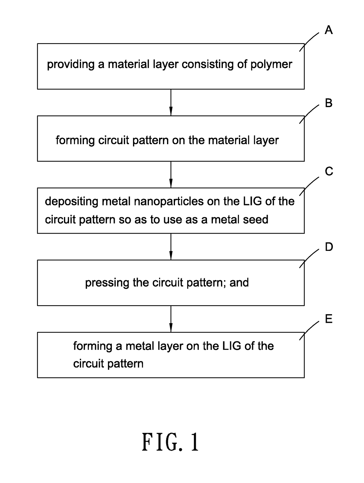
[0033]With reference to FIG. 1, a method of manufacturing a polymer printed circuit board according to the present invention comprises steps of:

[0034]A. providing a material layer 10 consisting of polymer;

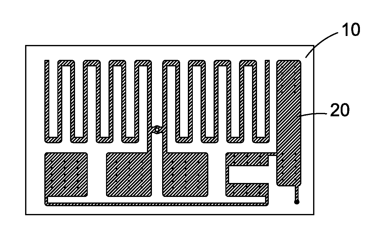
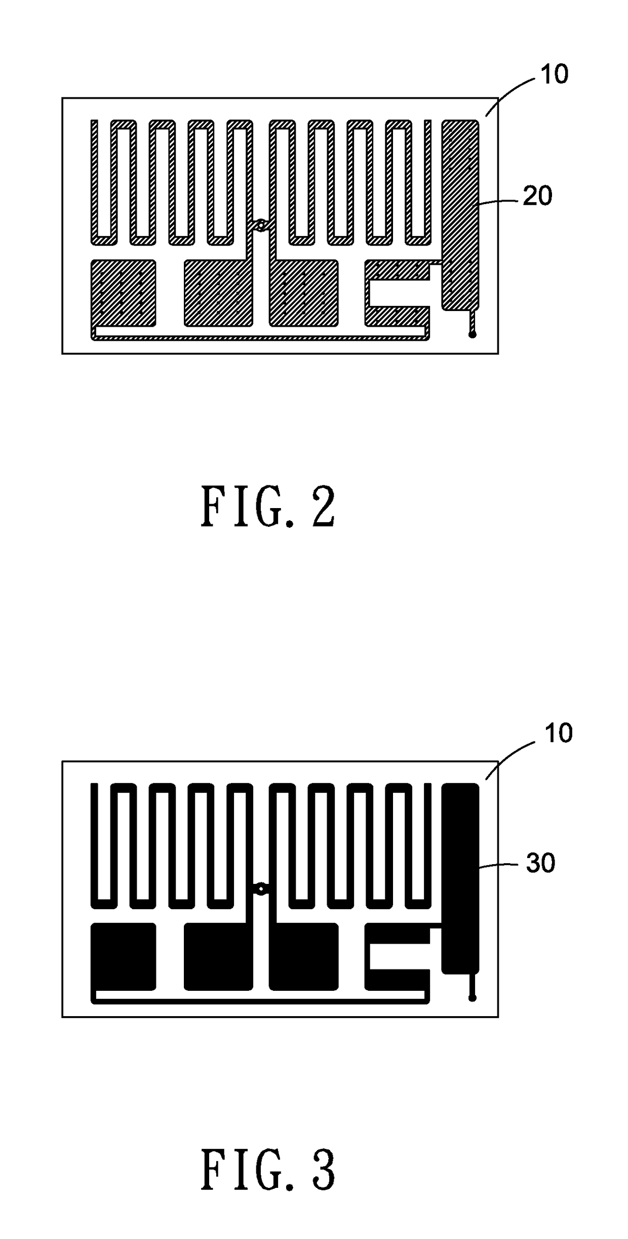
[0035]B. forming circuit pattern on the material layer 10, wherein the circuit pattern is comprised of laser induced graphene (LIG) 20, as shown in FIG. 2;

[0036]C. depositing metal nanoparticles on the LIG 20 of the circuit pattern so as to use as a metal seed;

[0037]D. pressing the circuit pattern; and

[0038]E. forming a metal layer 30 on the LIG 20 of the circuit pattern, as illustrated in FIG. 3.

[0039]The material layer 10 is a polymer film or a substrate on which the polymer is coated. Preferably, the polymer is selected from the group of polyimide (PI) and polyetherimide (PEI).

[0040]The LIG 20 is formed on the material layer 10 in a laser induction reacting process which is controlled by a computer.

[0041]Preferably, the material layer 10 is a smooth surface, and the computer con...

second embodiment

[0044]Referring to FIG. 4, a method of manufacturing a polymer printed circuit board according to the present invention comprises steps of:

[0045]A. providing a material layer 10 consisting of polymer;

[0046]B. forming circuit pattern on the material layer 10, wherein the circuit pattern is comprised of laser induced graphene (LIG) 20;

[0047]C. depositing metal nanoparticles on the LIG 20 of the circuit pattern so as to use as a metal seed;

[0048]D. forming a metal layer 30 on the LIG 20 of the circuit pattern; and

[0049]E. pressing the circuit pattern on which the metal layer 30 is formed.

[0050]Thereby, the circuit pattern is adhered on the material layer 10 securely and has outstanding electric conductivity after being pressed in the step E.


PUM

PropertyMeasurementUnit
Temperatureaaaaaaaaaa
Electrical conductivityaaaaaaaaaa

Abstract

A method of manufacturing a polymer printed circuit board contains steps of: A. providing a material layer consisting of polymer; B. forming circuit pattern on the material layer; C. depositing metal nanoparticles on the LIG of the circuit pattern so as to use as a metal seed; D. pressing the circuit pattern; and E. forming a metal layer on the LIG of the circuit pattern. In the step of B, the circuit pattern includes laser induced graphene, and the laser induced graphene is porous. Thereby, the circuit pattern is adhered on the material layer securely and has outstanding electric conductivity after being pressed in the step D.

Description

FIELD OF THE INVENTION[0001]The present invention relates to a method of manufacturing a printed circuit board, and more particular to a method of manufacturing a polymer printed circuit board.BACKGROUND OF THE INVENTION[0002]Methods of manufacturing printed circuit board (PCB) contain a subtractive method and a semi-additive method, etc. However, the subtractive method pollutes environment and increases production cost. As using the semi-additive method, cooper is etched decreasingly in deposition process.[0003]As using the subtractive method to manufacture a printed circuit board which includes a copper clad laminate (CCL), and the CCL has a polymer substrate, a glass fiber, and a copper foil, wherein the copper foil is fixed on the polymer substrate and a main part of the copper foil is etched or eliminated. However, water consumption increases greatly as etching the copper foil in photolithography process and in rinsing process. Furthermore, chemical waste and heavy metals produ...

Claims


Application Information

Patent Timeline
IPC IPC(8): H05K3/10H05K1/09H05K1/03H05K3/16H05K3/18
CPCH05K3/108H05K1/092H05K1/0346H05K3/16H05K2201/0129H05K2201/0323H05K2203/107H05K2203/06H05K2201/0154H05K3/18H05K3/182H05K3/188H05K3/381H05K3/388H05K2201/0257
Inventor CHANG, KUO-HSINCHEN, JIA-CINGKE, WE-JEIZHANG, JINGYULAI, CHUNG-PING
Owner BGT MATERIALS
Why Eureka
Try Eureka