Solid-state image sensor, driving method, and electronic apparatus

a solid-state image sensor and driving method technology, applied in the direction of color television, television system, radio control device, etc., can solve the problems of reducing the signal-to-noise ratio, difficult to prepare the region enough to install a pd, etc., and achieve the effect of improving sensitivity and reducing pixel siz

Active Publication Date: 2018-07-26
SONY CORP
View PDF12 Cites 5 Cited by
  • Summary
  • Abstract
  • Description
  • Claims
  • Application Information

AI Technical Summary

Benefits of technology

[0014]According to an embodiment of the present disclosure, it is possible to achieve reduction in pixel size and sensitivity improvement.

Problems solved by technology

Further, as the size of a pixel become smaller, there has been concern that a region enough to install a PD is very difficult to be prepared and the signal-to-noise (SN) ratio is decreased, and so techniques for increasing the volume of a PD have been developed.

Method used


Image

  • Solid-state image sensor, driving method, and electronic apparatus
  • Solid-state image sensor, driving method, and electronic apparatus
  • Solid-state image sensor, driving method, and electronic apparatus

Examples


Embodiment Construction

[0047]A specific embodiment to which the present technology is applied is now described in detail with reference to the drawings.

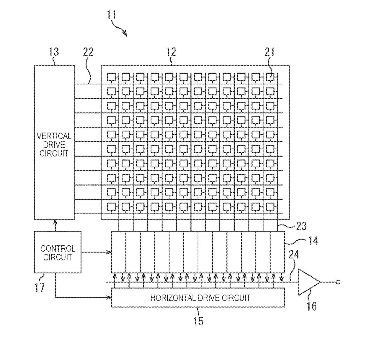
[0048]FIG. 1 is a block diagram illustrating a configuration example of an embodiment of an image sensor to which the present technology is applied.

[0049]As illustrated in FIG. 1, an image sensor 11 includes a pixel region 12, a vertical drive circuit 13, a column signal processing circuit 14, a horizontal drive circuit 15, an output circuit 16, and a control circuit 17.

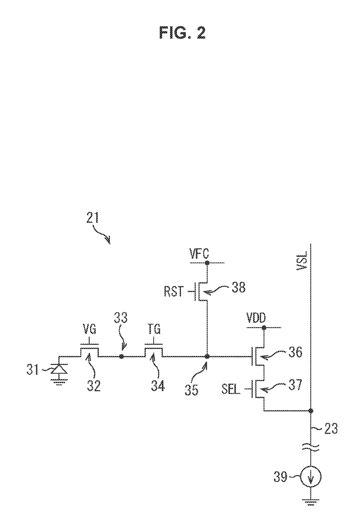
[0050]The pixel region 12 is a light receiving surface that receives light collected by an optical system (not illustrated). In the pixel region 12, a plurality of pixels 21 are arranged in a matrix form, and each of the pixels 21 is connected to the vertical drive circuit 13 row by row through a horizontal signal line 22 and is connected to the column signal processing circuit 14 column by column through a vertical signal line 23. Each of the plurality of pixels 21 output a pixel signal at...


PUM


Abstract

The present disclosure relates to a solid-state image sensor, driving method, and electronic apparatus, capable of achieving reduction in pixel size and sensitivity improvement. The solid-state image sensor includes a PD configured to convert light into electric charge by photoelectric conversion and to store the electric charge, a first transfer transistor configured to read out the electric charge stored in the photoelectric conversion unit, a multiplication region configured to store temporarily and multiply the electric charge read out through the read-out unit, and a second transfer transistor configured to transfer the electric charge stored in the multiplication region to a conversion unit configured to convert the electric charge into a pixel signal. Then, an intense electric field is generated in the multiplication region to multiply electric charge by the avalanche effect in transferring the electric charge from the multiplication region to an FD portion through the second transfer transistor. The present technology is applicable to, in one example, the stacked CMOS image sensors.

Description

TECHNICAL FIELD[0001]The present disclosure relates to a solid-state image sensor, a driving method, and an electronic apparatus, and in particular, to a solid-state image sensor, driving method, and electronic apparatus, capable of achieving reduction in pixel size and sensitivity improvement.BACKGROUND ART[0002]In the related art, in an electronic apparatus, such as digital still cameras or digital video cameras, equipped with an image capture function, in one example, a solid-state image sensor such as charge-coupled device (CCD) or complementary metal-oxide-semiconductor (CMOS) image sensor has been used. The solid-state image sensor has a pixel in which a photodiode (PD) that performs photoelectric conversion and a plurality of transistors are combined, and an image is constructed on the basis of pixel signals that are output from a plurality of pixels arranged on an image plane on which an image of a photographic subject is formed.[0003]Further, as the size of a pixel become s...

Claims


Application Information

Patent Timeline
Patent Type & Authority Applications(United States)
IPC IPC(8): H04N5/378H04N5/372H04N5/3745
CPCH04N5/378H04N5/37206H04N5/37455H01L27/14609H01L27/14623H01L27/14647H04N25/778H04N25/771H04N25/75H01L27/146H01L31/107H01L31/10H04N25/79H04N25/711H04N25/772
Inventor SANO, TAKUYA
Owner SONY CORP
Why Eureka
Try Eureka